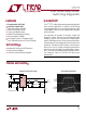
LT1777 Low Noise Step-Down Switching Regulator U FEATURES ■ ■ ■ ■ ■ ■ ■ ■ ■ DESCRIPTIO The LT ®1777 is a Buck (step-down) regulator designed for noise sensitive applications. It contains a dI/dt limiting circuit programmed via a small external inductor in the switching path. Internal circuitry also generates controlled dV/dt ramp rates.
LT1777 W U U U W W W ABSOLUTE MAXIMUM RATINGS PACKAGE/ORDER I FOR ATIO (Note 1) Supply Voltage ....................................................... 48V Switch Voltage (VIN – VSW) (Note 4) ...................... 51V SHDN, SYNC Pin Voltage .......................................... 7V VCC Pin Voltage ...................................................... 30V FB Pin Voltage ........................................................ 3.0V Operating Junction Temperature Range LT1777C ...................
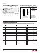
LT1777 ELECTRICAL CHARACTERISTICS The ● denotes specifications which apply over the full operating temperature range, otherwise specifications are at TJ = 25°C. VIN = 24V, VSW Open, VCC = 5V, VC = 1.4V unless otherwise noted. SYMBOL PARAMETER CONDITIONS MIN TYP MAX UNITS 1.0 1.5 V 0.70 1.0 A 2.0 V V Output Switch RON Output Switch On Voltage ISW = 0.5A ILIM Switch Current Limit (Note 3) ● 0.55 Output dl/dt Sense Voltage 1.3 ● 0.
LT1777 U W TYPICAL PERFOR A CE CHARACTERISTICS Switch On Voltage vs Switch Current 7.4 1.50 7.2 1.25 SWITCH VOLTAGE (V) INPUT VOLTAGE (V) Minimum Input Voltage vs Temperature 7.0 6.8 6.6 6.4 25°C – 55°C 1.00 0.75 125°C 0.50 0.25 6.2 6.
LT1777 U W TYPICAL PERFOR A CE CHARACTERISTICS Switching Frequency vs Temperature Minimum Synchronization Voltage vs Temperature MINIMUM SYNCHRONIZATION VOLTAGE (V) SWITCHING FREQUENCY (kHz) 106 104 102 100 98 96 94 –50 –25 0 25 50 75 100 2.25 2.00 1.75 1.50 1.25 1.00 0.75 –50 –25 125 TEMPERATURE (°C) 0 25 50 75 100 1777 G07 1777 G08 VC Pin Switching Threshold, Clamp Voltage vs Temperature 2.0 2.2 1.8 2.0 1.6 1.
LT1777 U U U PIN FUNCTIONS GND (Pins 1, 8, 9, 16): These corner package pins are mechanically connected to the die paddle and thus aid in conducting away internally generated heat. As these are electrically connected to the die substrate, they must be held at ground potential. A direct connection to the local ground plane is recommended. NC (Pins 2, 11, 15): Package Pins 2, 11 and 15 are unconnected. SHDN (Pin 3): When pulled below the shutdown mode threshold, nominally 0.
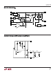
LT1777 W BLOCK DIAGRA 4 3 12 7 14 13 VIN VCC SHDN SYNC R1 VB BIAS 10 RSENSE VBG OSC LOGIC – dV/dt LIMITER ICOMP SWDR Q2 SWON Q1 SGND VSW VC I 6 I1 FEEDBACK AMP FB gm I VD ± dI/dt LIMITER I2 VBG 5 1777 BD W W OUTPUT STAGE SI PLIFIED SCHE ATIC VIN C1 Q2 Q3 R1 Q4 R2 Q6 Q1 VSW I1 I LSENSE SWITCH ON SIGNAL LMAIN VOUT + R3 Q5 R4 VD NOTE: R3 = R4 1777 SS 7
LT1777 U OPERATIO The LT1777 is a current mode step-down switcher regulator IC designed for low noise operation. The Block Diagram shows an overall view of the system. The individual blocks are straightforward and similar to those found in traditional designs, including: Internal Bias Regulator, Oscillator, Logic, and Feedback Amplifier. The novel portion includes a specialized Output Switch section including circuits to limit the dI/dt and dV/dt switching rates.
LT1777 U W U U APPLICATIONS INFORMATION Basics of Low Noise Operation Switching power supply circuits are often preferred over linear topologies for their improved efficiency (POUT/ PIN). However, their typically rapid voltage and current slew rates often cause “radio frequency” interference problems, commonly referred to as “RFI”.
LT1777 U W U U APPLICATIONS INFORMATION The question is “What is the allowed range of values for a sense inductor in a given application?” There is really no minimum limit to the sense inductor, i.e., its value is allowed to be zero. (In other words, the physical sense inductor ceases to exist and is replaced by a short circuit.) This will yield the highest efficiency possible in a given situation.
LT1777 U U W U APPLICATIONS INFORMATION current waveform. The four sense inductor values of 0µH, 0.47µH, 1µH and 2.2µH yield dI/dt rates of roughly 4.5A/µs, 2.2A/µs, 1.4A/µs and 0.6A/µs, respectively. These photos show that there is a minimum effective value for sense inductance, which is 0.47µH for a typical part at room temperature as shown. This value inductor has a small effect on the trailing edge rate, but essentially no effect on the rising edge.
LT1777 U W U U APPLICATIONS INFORMATION 10dB/DIV voltage of 12V, and then 36V. Once again the circuit is the Typical Application shown on the first page of this data sheet, with an output load of 400mA. 1777 F04a 0MHz to 20MHz (2MHz/DIV) (a) LT1676 for Comparison Figure 5a, with VIN of 12V, shows a relatively rectangular voltage waveform. The limited voltage slew rate still allows for nearly vertical switching edges, so little power is wasted.
LT1777 U W U U APPLICATIONS INFORMATION 10V/DIV through the main inductor has most of its energy concentrated in the fundamental and lower harmonics.) Toroidal style inductors, many available in surface mount configuration, offer a reduced external magnetic field, generally at an increase in cost and physical size. Although custom design is always a possibility, most potential LT1777 applications can be handled by the array of standard, off-theshelf inductor products offered by the major suppliers.
LT1777 U W U U APPLICATIONS INFORMATION Maximum Load/Short-Circuit Considerations The LT1777 is a current mode controller. It uses the VC node voltage as an input to a current comparator, which turns off the output switch on a cycle-by-cycle basis as this peak current is reached. The internal clamp on the VC node, nominally 2.0V, then acts as an output switch peak current limit. This action becomes the switch current limit specification.
LT1777 U W U U APPLICATIONS INFORMATION However, remember that oscillator slowdown to achieve short-circuit protection (discussed above) is dependent on FB pin behavior, and this in turn, is sensitive to FB node external impedance. The graph in Figure 7 shows the typical relationship between FB pin voltage, driving impedance and oscillator frequency.
LT1777 U W U U APPLICATIONS INFORMATION As an example, assume that the capacitance between the VSW node and a high impedance pin node is 0.1pF, and that the high impedance node in question exhibits a capacitance of 1pF to ground. Also assume a “typical” 36VIN to 5VOUT application. Due to the large voltage excursion at the VSW node, this will couple a 3.5V(!) transient to the high impedance pin, causing abnormal operation.
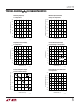
LT1777 U TYPICAL APPLICATIONS output current should not present a problem, though.) As shown, the SHDN and SYNC pins are unused, however either (or both) can be optionally driven by external signals as desired. Basic 5V Output Application Figure 8 shows a basic application that produces 5V at up to 500mA IOUT. Efficiency and Internal Power Dissipation graphs are shown in Figure 9 for input voltages of 12V, 24V and 36V, and for sense inductor values of 0µH, 1µH and 2.2µH.
LT1777 U TYPICAL APPLICATIONS Efficiency 80 EFFICIENCY (%) VIN = 12V VOUT = 5V TA = 25°C 1.2 1µH 70 VIN = 12V 1.4 LSENSE = 0µH VIN = 12V VOUT = 5V TA = 25°C 2.2µH 60 50 40 INTERNAL DISSIPATION (W) 90 Internal Dissipation 30 1.0 LSENSE = 2.2µH 0.8 1µH 0µH 0.6 0.4 0.2 20 10 1 100 0 1000 10 1000 100 IOUT (mA) ILOAD (mA) 1777 F09a 1.4 VIN = 24V VOUT = 5V TA = 25°C 80 LSENSE = 0µH VIN = 24V EFFICIENCY (%) 70 1µH 60 2.2µH 50 40 30 LSENSE = 2.
LT1777 U TYPICAL APPLICATIONS Basic 3.3V Output Application dissipation is largely determined by input voltage, load current and sense inductor, and is only a weak function of output voltage. Figure 10 shows a circuit similar to the previous example, but modified for a 3.3V output. Once again, Efficiency and Internal Power Dissipation graphs are shown in Figure 11 for input voltages of 12V, 24V and 36V, and for sense inductor values of 0µH, 1µH and 2.2µH.
LT1777 U TYPICAL APPLICATIONS Efficiency 1.4 VIN = 12V VOUT = 3.3V TA = 25°C 80 LSENSE = 0µH VIN = 12V EFFICIENCY (%) 70 1.2 1µH 60 2.2µH 50 40 INTERNAL DISSIPATION (W) 90 Internal Dissipation 30 VIN = 12V VOUT = 3.3V TA = 25°C 1.0 LSENSE = 2.2µH 0.8 0.6 1µH 0µH 0.4 0.2 20 10 1 100 0 1000 10 ILOAD (mA) 1000 100 IOUT (mA) 1777 F11a 1.4 VIN = 24V VOUT = 3.3V TA = 25°C 80 1.2 LSENSE = 0µH VIN = 24V EFFICIENCY (%) 70 60 1µH 50 2.
LT1777 U TYPICAL APPLICATIONS Optional Input/Output Filtering When minimum conducted noise is required, it is often advantageous to add an explicit input and/or output filter to the topology. This can be a cost-effective way to reduce conducted noise on the input or output node by an order of magnitude or more. The exact details involved are a bit lengthy, so the user is referred to the thorough treatments in Application Notes AN19 and AN44.
LT1777 U TYPICAL APPLICATIONS VOUT NODE AC COUPLED 2mV/DIV VOUT NODE AC COUPLED 2mV/DIV 1777 F13a 1777 F14b 2µs/DIV 2µs/DIV (a) Before Output Filter (b) After Output Filter Figure 14. Output Node Ripple User Programmable Undervoltage Lockout Figure 15 uses a resistor divider between VIN and ground to drive the SHDN node. This is a simple, cost-effective way to add a user-programmable undervoltage lockout (UVLO) function.
LT1777 U PACKAGE DESCRIPTION Dimensions in inches (millimeters) unless otherwise noted. S Package 16-Lead Plastic Small Outline (Narrow 0.150) (LTC DWG # 05-08-1610) 0.386 – 0.394* (9.804 – 10.008) 16 15 14 13 12 11 10 9 0.150 – 0.157** (3.810 – 3.988) 0.228 – 0.244 (5.791 – 6.197) 1 0.010 – 0.020 × 45° (0.254 – 0.508) 2 3 4 5 6 0.053 – 0.069 (1.346 – 1.752) 0.008 – 0.010 (0.203 – 0.254) 0.014 – 0.019 (0.355 – 0.483) TYP 8 0.004 – 0.010 (0.101 – 0.254) 0° – 8° TYP 0.016 – 0.050 (0.
LT1777 U TYPICAL APPLICATION Minimum PC Board Size Application circuit is capable of delivering up to 300mA at 5V, from input voltages as high as 28V. The only disadvantage is that due to the increased resistance in the inductor, the circuit is no longer capable of withstanding indefinite short circuits to ground. The LT1777 will still current limit at its nominal ILIM value, but this will overheat the inductor. Momentary short circuits of a few seconds or less can still be tolerated.