
Datasheet


3
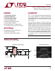
LT1777
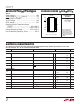
ELECTRICAL CHARACTERISTICS
Note 1: Absolute Maximum Ratings are those values beyond which the life
of a device may be impaired.
Note 2: Control circuitry powered from V
CC
.
Note 3: Switch current limit is DC trimmed and tested in production.
Inductor dI/dt rate will cause a somewhat higher current limit in actual
application.
Note 4: During normal operation the V
SW
pin may fly as much as 3V
below ground. However, the LT1777 may not be used in an inverting
DC/DC configuration.
SYMBOL PARAMETER CONDITIONS MIN TYP MAX UNITS
Output Switch
R
ON
Output Switch On Voltage I
SW
= 0.5A 1.0 1.5 V
I
LIM
Switch Current Limit (Note 3) ● 0.55 0.70 1.0 A
Output dl/dt Sense Voltage 1.3 V
● 0.6 2.0 V
Current Amplifier
Control Pin Threshold Duty Cycle = 0% 0.9 1.1 1.25 V
Control Voltage to Switch Transconductance 2 A/V
Timing
f Switching Frequency 90 100 110 kHz
● 85 115 kHz
Maximum Switch Duty Cycle ● 85 90 %
Sync Function
Minimum Sync Amplitude ● 1.5 2.2 V
Synchronization Range ● 130 250 kHz
SYNC Pin Input R 40 kΩ
SHDN Pin Function
V
SHDN
Shutdown Mode Threshold 0.5 V
● 0.2 0.8 V
Upper Lockout Threshold Switching Action On 1.260 V
Lower Lockout Threshold Switching Action Off 1.245 V
I
SHDN
Shutdown Pin Current V
SHDN
= 0V 12 20 µA
V
SHDN
= 1.25V 2.5 10 µA
The ● denotes specifications which apply over the full operating temperature range, otherwise specifications are at T
J
= 25°C.
V
IN
= 24V, V
SW
Open, V
CC
= 5V, V
C
= 1.4V unless otherwise noted.