
Datasheet


6
LT1777
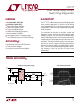
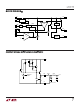
PIN FUNCTIONS
UUU
removed or supplied accordingly to limit dI/dt (see Appli-
cations Information).
V
SW
(Pin 6): This is the emitter node of the output switch
and has large currents flowing through it. Keep the traces
to the switching components as short as possible to
minimize electromagnetic radiation and voltage spikes.
SGND (Pin 7): This is the device signal ground pin. The
internal reference and feedback amplifier are referred to it.
Keep the ground path connection to the FB divider and the
V
C
compensation capacitor free of large ground currents.
V
IN
(Pin 10): This is the high voltage supply pin for the
output switch. It also supplies power to the internal control
circuitry during start-up conditions or if the V
CC
pin is left
open. A high quality bypass capacitor which meets the
input ripple current requirements is needed here (see
Applications Information).
SYNC (Pin 12): Pin to synchronize internal oscillator to
external frequency reference. It is directly logic compat-
ible and can be driven with any signal between 10% and
90% duty cycle. The sync function is internally disabled if
the FB pin voltage is low enough to cause oscillator
slowdown. If unused, this pin should be grounded.
FB (Pin 13): This is the inverting input to the feedback
amplifier. The noninverting input of this amplifier is inter-
nally tied to the 1.24V reference. This pin also slows down
the frequency of the internal oscillator when its voltage is
abnormally low, e.g. 2/3 of normal or less. This feature
helps maintain proper short-circuit protection. Coupling
from high speed noise to this pin can cause irregular
operation. (See Switch Node Considerations section.)
V
C
(Pin 14): This is the control voltage pin which is the
output of the feedback amplifier and the input of the
current comparator. Frequency compensation of the over-
all loop is effected by placing a capacitor (or in most cases
a series R/C combination) between this node and ground.
Coupling from high speed noise to this pin can cause
irregular operation. (See Switch Node Considerations
section.)
GND (Pins 1, 8, 9, 16): These corner package pins are
mechanically connected to the die paddle and thus aid in
conducting away internally generated heat. As these are
electrically connected to the die substrate, they must be
held at ground potential. A direct connection to the local
ground plane is recommended.
NC (Pins 2, 11, 15): Package Pins 2, 11 and 15 are
unconnected.
SHDN (Pin 3): When pulled below the shutdown mode
threshold, nominally 0.5V, this pin turns off the regulator
and reduces V
IN
input current to a few tens of microam-
peres (shutdown mode).
When this pin is held above the shutdown mode threshold,
but below the lockout threshold, the part will be opera-
tional with the exception that output switching action will
be inhibited (lockout mode). A user-adjustable undervolt-
age lockout can be implemented by driving this pin from
an external resistor divider to V
IN
. This action is logically
“ANDed” with the internal UVLO, nominally set at 6.7V,
such that minimum V
IN
can be increased above 6.7V, but
not decreased (see Applications Information).
If unused, this pin should be left open. However, the high
impedance nature of this pin renders it susceptible to
coupling from the V
SW
node, so a small capacitor to
ground, typically 100pF or so is recommended when the
pin is left open.
V
CC
: (Pin 4): Pin to power the internal control circuitry
from the switching supply output. Proper use of this pin
enhances overall power supply efficiency. During start-up
conditions, internal control circuitry is powered directly
from V
IN
. If the output capacitor is located more than an
inch from the V
CC
pin, a separate 0.1µF bypass capacitor
to ground may be required right at the pin.
V
D
(Pin 5): This pin is used in conjunction with a small
external sense inductor to limit power path dI/dt. The
sense inductor is placed between the V
SW
output node and
the cathode of the freewheeling (power) diode, and the V
D
pin is connected to the diode. As the voltage across the
inductor reaches ±2V
BE
, drive to the output transistor is