
Datasheet


LT1785/LT1785A/
LT1791/LT1791A
7
178591fc
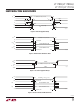
PIN FUNCTIONS
RO: Receiver Output. TTL level logic output. If the receiver
is active (RE pin low), RO is high if receiver input A ≥ B
by 200mV. If A ≤ B by 200mV, then RO will be low. RO
assumes a high impedance output state when RE is high
or the part is powered off. RO is protected from output
shorts from ground to 6V.
RE: Receiver Output Enable. TTL level logic input. A logic
low on RE enables normal operation of the receiver output
RO. A logic high level at RE places the receiver output pin
RO into a high impedance state. If receiver enable RE and
driver enable DE are both in the disable state, the circuit-
goes to a low power shutdown state. Placing either RE or
DE into its active state brings the circuit out of shutdown.
Shutdown state is not entered until a 3µs delay after both
RE and DE are disabled, allowing for logic skews in tog-
gling between transmit and receive modes of operation.
For CAN bus applications, RE should be tied low to prevent
the circuit from entering shutdown.
DE: Driver Output Enable. TTL level logic input. A logic
high on DE enables normal operation of the driver out-
puts (Y and Z on LT1791, A and B on LT1785). A logic
low level at DE places the driver output pins into a high
impedance state. If receiver enable RE and driver enable
DE are both in the disable state, the circuit goes to a low
power shutdown state. Placing either RE or DE into its
active state brings the circuit out of shutdown. Shutdown
state is not entered until a 3µs delay after both RE and DE
are disabled, allowing for logic skews in toggling between
transmit and receive modes of operation. For CAN bus
operation the DE pin is used for signal input to place the
data bus in dominant or recessive states.
DI: Driver Input. TTL level logic input. A logic high at DI
causes driver output A or Y to a high state, and output B
or Z to a low state. Complementary output states occur for
DI low. For CAN bus applications DI should be tied low.
GND: Ground.
Y: Driver Output. The Y driver output is in phase with the
driver input DI. In the LT1785 driver output Y is internally
connected to receiver input A. The driver output assumes
a high impedance state when DE is low, power is off or
thermal shutdown is activated. The driver output is pro-
tected from shorts between ±60V in both active and high
impedance modes. For CAN applications, output Y is the
CANL output node.
Z: Driver Output. The Z driver output is opposite in phase
to the driver input DI. In the LT1785 driver output Z is
internally connected to receiver input B. The driver output
assumes a high impedance state when DE is low, power
is off or thermal shutdown is activated. The driver output
is protected from shorts between ±60V in both active and
high impedance modes. For CAN applications, output Z is
the CANH output node.
A: Receiver Input. The A receiver input forces a high receiver
output when V(A) ≥ [V(B) + 200mV]. V(A) ≤ [V(B)– 200mV]
forces a receiver output low. Receiver inputs A and B are
protected against voltage faults between ±60V. The high
input impedance allows up to 128 LT1785 or LT1791
transceivers on one RS485 data bus.
The LT1785A/LT1791A have guaranteed receiver input
thresholds –200mV < V
TH
< 0. Receiver outputs are
guaranteed to be in a high state for 0V inputs.
B: Receiver Input. The B receiver input forces a high
receiver output when V(A) ≥ [V(B) + 200mV]. When
V(A) ≤ [V(B) – 200mV], the B receiver forces a receiver
output low. Receiver inputs A and B are protected against
voltage faults between ±60V. The high input impedance
allows up to 128 LT1785 or LT1791 transceivers on one
RS485 data bus.
The LT1785A/LT1791A have guaranteed receiver input-
thresholds –200mV < V
TH
< 0. Receiver outputs are
guaranteed to be in a high state for 0V inputs.
V
CC
: Positive Supply Input. For RS422 or RS485 operation,
4.75V ≤ V
CC
≤ 5.25V. Higher V
CC
input voltages increase
output drive swing. V
CC
should be decoupled with a 0.1µF
low ESR capacitor directly at Pin 8 (V
CC
).