
Datasheet


LT1785/LT1785A/
LT1791/LT1791A
5
178591fc
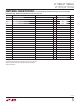
SWITCHING CHARACTERISTICS
The l denotes the specifi cations which apply over the full operating
temperature range, otherwise specifi cations are at T
A
= 25°C, V
CC
= 5V.
SYMBOL PARAMETER CONDITIONS MIN TYP MAX UNITS
t
PLH
Driver Input to Output Figures 3, 5
l
700 2000 ns
t
PHL
Driver Input to Output Figures 3, 5
l
700 2000 ns
t
SKEW
Driver Output to Output Figures 3, 5 100 ns
t
r
, t
f
Driver Rise or Fall Time Figures 3, 5
l
200 800 2000 ns
t
ZH
Driver Enable to Output High Figures 4, 6
l
500 3000 ns
t
ZL
Driver Enable to Output Low Figures 4, 6
l
800 3000 ns
t
LZ
Driver Disable Time from Low Figures 4, 6
l
200 5000 ns
t
HZ
Driver Disable Time from High Figures 4, 6
l
800 5000 ns
t
PLH
Receiver Input to Output Figures 3, 7
l
400 900 ns
t
PHL
Receiver Input to Output Figures 3, 7
l
400 900 ns
t
SKD
Differential Receiver Skew 200 ns
t
ZL
Receiver Enable to Output Low Figures 2, 8
l
300 1000 ns
t
ZH
Receiver Enable to Output High Figures 2, 8
l
300 1000 ns
t
LZ
Receiver Disable from Low Figures 2, 8
l
400 1000 ns
t
HZ
Receiver Disable from High Figures 2, 8
l
400 1000 ns
f
MAX
Maximum Data Rate
l
250 kbps
t
SHDN
Time to Shut Down Figures 2, 6, 8 3 µs
t
ZH(SHDN)
Driver Enable from Shutdown to Output High Figures 2, 6; RE = 5V 12 µs
t
ZL(SHDN)
Driver Enable from Shutdown to Output Low Figures 2, 6; RE = 5V 12 µs
t
ZH(SHDN)
Receiver Enable from Shutdown to Output High Figures 2, 8; DE = 0V 4 µs
t
ZL(SHDN)
Receiver Enable from Shutdown to Output Low Figures 2, 8; DE = 0V 4 µs
Note 1: Stresses beyond those listed under Absolute Maximum Ratings
may cause permanent damage to the device. Exposure to any Absolute
Maximum Rating condition for extended periods may affect device
reliability and lifetime.