
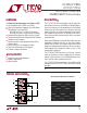
Datasheet

8
LT1785/LT1785A
LT1791/LT1791A
Overvoltage Protection
The LT1785/LT1791 RS485/RS422 transceivers answer
an applications need for overvoltage fault tolerance on
data networks. Industrial installations may encounter
common mode voltages between nodes far greater than
the –7V to 12V range specified for compliance to RS485
standards. CMOS RS485 transceivers can be damaged by
voltages above their absolute maximum ratings of typi-
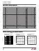
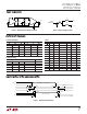
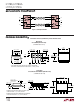
SWITCHI G TI E WAVEFOR S
UW W
Figure 8. Receiver Enable and Disable Times
Figure 7. Receiver Propagation Delays
Figure 6. Driver Enable and Disable Times
1.5V
2.3V
2.3V
t
ZH(SHDN)
,
t
ZH
t
ZL(SHDN)
,
t
ZL
1.5V
t
LZ
0.5V
0.5V
t
HZ
OUTPUT NORMALLY LOW
OUTPUT NORMALLY HIGH
5V
0V
DE
5V
V
OL
V
OH
0V
A, B
A, B
1785/91 F06
f = 125kHz, t
r
≤ 10ns, t
f
≤ 10ns
1.5V
t
PHL
RO
–V
OD2
A – B
0V 0V
1.5V
t
PLH
OUTPUT
INPUT
V
OD2
V
OL
V
OH
1785/91 F07
f = 125kHz, t
r
≤ 10ns, t
f
≤ 10ns
1.5V
t
ZL(SHDN)
, t
ZL
t
ZH(SHDN)
, t
ZH
1.5V
1.5V
1.5V
t
LZ
0.5V
0.5V
t
HZ
OUTPUT NORMALLY LOW
OUTPUT NORMALLY HIGH
5V
0V
RE
5V
0V
RO
RO
1785/91 F08
f = 125kHz, t
r
≤ 10ns, t
f
≤ 10ns
APPLICATIO S I FOR ATIO
UU W U
cally –8V to 12.5V. Replacement of standard RS485
transceiver components with the LT1785 or LT1791
devices eliminates field failures due to overvoltage faults
or the use of costly external protection devices. The limited
overvoltage tolerance of CMOS RS485 transceivers makes
implementation of effective external protection networks
difficult without interfering with proper data network
performance within the –7V to 12V region of RS485
operation.