
Datasheet


LT1789-1/LT1789-10
8
1789fb
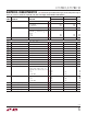
SYMBOL PARAMETER CONDITIONS
LT1789-1 LT1789-10
UNITSMIN TYP MAX MIN TYP MAX
PSRR Power Supply Rejection Ratio
LT1789-1, V
S
= ±1.25V to ±16V
LT1789-10, V
S
= ±1.50V to ±16V
G = 1
G = 10
G = 100, 1000
l
l
l
92
102
104
98
104
dB
dB
dB
Minimum Supply Voltage
l
±1.25 ±1.50 V
I
S
Supply Current
l
150 150 µA
V
O
Output Voltage Swing
l
±14.25 ±14.25 V
SR Slew Rate V
OUT
= ±10V
l
0.010 0.026 V/µs
ELECTRICAL CHARACTERISTICS
The l denotes the specifi cations which apply over the temperature range of
0°C ≤ T
A
≤ 70°C. V
S
= ±15V, R
L
= 20k, V
CM
= V
REF
= 0V, unless otherwise noted. (Note 4)
The l denotes the specifi cations which apply over the temperature range of –40°C ≤ T
A
≤ 85°C. V
S
= ±15V, R
L
= 20k, V
CM
= V
REF
= 0V,
unless otherwise noted. (Note 4)
SYMBOL PARAMETER CONDITIONS
LT1789-1 LT1789-10
UNITSMIN TYP MAX MIN TYP MAX
Gain Error V
O
= ±10V
G = 1
G = 10 (Note 2)
G = 100 (Note 2)
G = 1000 (Note 2)
l
l
l
l
0.20
0.57
0.57
0.62
0.25
0.62
0.67
%
%
%
%
Gain Nonlinearity V
O
= ±10V
G = 1
G = 10
G = 100
G = 1000
l
l
l
l
30
20
30
130
50
50
200
ppm
ppm
ppm
ppm
G/T Gain vs Temperature G < 1000 (Notes 2, 3)
l
5 50 5 50 ppm/°C
V
OST
Total Input Referred Offset Voltage V
OST
= V
OSI
+ V
OSO
/G
V
OSI
Input Offset Voltage G = 1000
l
305
340
µV
V
OSIH
Input Offset Voltage Hysteresis (Notes 3, 5)
l
8 30 8 30 µV
V
OSO
Output Offset Voltage G = 1
l
1.3 4.2 mV
V
OSOH
Output Offset Voltage Hysteresis (Notes 3, 5)
l
50 120 400 1000 µV
V
OSI
/T Input Offset Voltage Drift (RTI) (Note 3)
l
0.2 0.7 0.3 0.8 µV/°C
V
OSO
/T Output Offset Voltage Drift (Note 3)
l
1.5
5 8 22 µV/°C
I
OS
Input Offset Current
l
55nA
I
OS
/T Input Offset Current Drift
l
2 2 pA/°C
I
B
Input Bias Current
l
50 50 nA
I
B
/T Input Bias Current Drift
l
35 35
pA/°C
V
CM
Input Voltage Range G = 1, Other Input Grounded
l
–14.8 14 –14.8 14 V
CMRR Common Mode Rejection Ratio
1k Source Imbalance,
V
CM
= –14.8V to 14V
G = 1
G = 10
G = 100, 1000
l
l
l
76
94
98
89
98
dB
dB
dB