
Datasheet


LT1790
19
1790fb
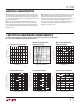
APPLICATIONS INFORMATION
Bypass and Load Capacitors
The LT1790 voltage references should have an input bypass
capacitor of 0.1μF or larger, however the bypassing of other
local devices may serve as the required component. These
references also require an output capacitor for stability.
The optimum output capacitance for most applications
is 1μF, although larger values work as well. This capaci-
tor affects the turn-on and settling time for the output to
reach its fi nal value.
All LT1790 voltages perform virtually the same, so the
LT1790-2.5 is used as an example.
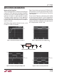
Figure 1 shows the turn-on time for the LT1790-2.5 with a
1μF input bypass and 1μF load capacitor. Figure 2 shows
the output response to a 0.5V transient on V
IN
with the
same capacitors.
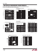
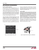
The test circuit of Figure 3 is used to measure the stability
of various load currents. With R
L
= 1k, the 1V step produces
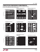
a current step of 1mA. Figure 4 shows the response to a
± 0.5mA load. Figure 5 is the output response to a sourcing
step from 4mA to 5mA, and Figure 6 is the output response
of a sinking step from –4mA to –5mA.
Figure 1. Turn-On Characteristics of LT1790-2.5
Figure 2. Output Response to 0.5V Ripple on V
IN
Figure 3. Response Time Test Circuit
Figure 4. LT1790-2.5 Sourcing and Sinking 0.5mA
Figure 5. LT1790-2.5 Sourcing 4mA to 5mA
LT1790-2.5
C
IN
0.1μF
C
L
1μF
V
GEN
1790 F03
1V
V
IN
3V
4
1, 2
1k
6
1790 F01
3V
V
IN
V
OUT
2V
0V
1V
1790 F02
3V
V
IN
V
OUT
2V
0V
1V
1790 F04
V
GEN
V
OUT
(AC COUPLED)
3V
2V
1790 F05
V
GEN
V
OUT
(AC COUPLED)
–3V
–2V