
Datasheet


LT1790
21
1790fb
APPLICATIONS INFORMATION
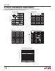
Figure 9. Worst-Case –40°C to 85°C Hysteresis on 80 Units
Figure 8. Worst-Case 0°C to 70°C Hysteresis on 79 Units
Hysteresis
Hysteresis data shown in Figures 8 and 9 represent the
worst-case data taken on parts from 0°C to 70°C and from
–40°C to 85°C. Units were cycled several times over these
temperature ranges and the largest change is shown. As
expected, the parts cycled over the higher temperature
range have higher hysteresis than those cycled over the
lower range.
In addition to thermal hysteresis, the thermal shock as-
sociated with high temperature soldering may cause the
output to shift. For traditional PbSn solder temperatures,
the output shift of the LT1790 is typically just 150ppm
(0.015%).
DISTRIBUTION (ppm)
–60 –50 –40 –30 –20 –10 0
10 20
30 40 50 60
NUMBER OF UNITS
1790 F08
30
20
0
10
25
15
5
70°C TO 25°C
0°C TO 25°C
DISTRIBUTION (ppm)
–100 –80 –60 –40 –20 0 20 40 60 80 100
NUMBER OF UNITS
20
25
30
1790 F09
15
10
0
5
50
45
40
–40°C TO 25°C
80°C TO 25°C
35
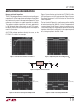
For lead-free solder, IR reflow temperatures are much
higher, often 240°C to 260°C at the peak. As a result, the
packaging materials have been optimized to reduce V
OUT
shift as possible during high temperature reflow. In addi-
tion, care should be taken when using lead-free solder to
minimize the peak temperature and dwell time as much
as is practical. A typical lead-free reflow profile is shown
in Figure 10. LT1790 units were heated using a similar
profile, with a peak temperature of 250°C. These parts
were run through the heating process 3 times to show the
cumulative effect of these heat cycles. Figure 11 shows
MINUTES
0246810
DEGREES (C)
150
120s
40s
t
L
130s
RAMP
DOWN
t
P
130s
1790 F10
75
0
300
225
380s
T
P
= 260°
T = 150°C
T = 190°C
T
S(MAX)
= 200°C
T
L
= 217°C
RAMP TO
150°C
Figure 10. Lead-Free Refl ow Profi le
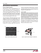
PPM
01020304050
NUMBER OF UNITS
4
5
6
1790 F11
3
2
0
1
9
8
7
Figure 11. 1X IR Refl ow Peak Temperature = 250°C,
Delta Output Voltage (ppm)