
Datasheet


LT1790
22
1790fb
APPLICATIONS INFORMATION
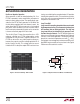
the shift after 1 cycle, while Figure 12 shows shift after
3 cycles. In the worst case, shifts are typically 150ppm,
but may be as high as 290ppm. Shifts in output voltage
are proportional to temperature and dwell time.
In general, the output shift can be reduced or fully recov-
ered by a long (12-24 hour) bake of the completed PC
Board assembly at high temperature (100°C to 150C°)
after soldering to remove mechanical stress that has been
induced by thermal shock. Once the PC Boards have cooled
to room temperature, they may continue to shift for up to
3 times the bake time. This should be taken into account
before any calibration is performed.
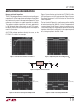
Assuming 80μA max supply current for the LT1790, a
25μA load, 120mV max dropout and a 4V to 30V input
specifi cation, the largest that R1 can be is (4V – 3.3V
– 120mV)/(80μA + 25μA) = 5.5k. Furthermore, assum-
ing 220mW of dissipation in the 18V SOT-23 Zener, this
gives a max current of (220mW)/(18V) = 12.2mA. So the
smallest that R1 should be is (30V – 18V)/12.2mA = 1k,
rated at 150mW.
With R1 = 1k, and assuming a 450mV worst-case drop-
out, the LT1790 can deliver a minimum current of (4V
– 3.3V–450mV)/(1k) = 250μA. In Figure 13, R1 and C1
provide fi ltering of the Zener noise when the Zener is in
its noisy V-I knee.
There are other variations for higher voltage operation that
use a pass transistor shown in Figures 14 and 15. These
circuits allow the input voltage to be as high as 160V while
maintaining low supply current.
LT1790-3.3
4V TO 30V
C1
0.1μF
BZX84C18
1μF
V
OUT
R1
1790 F13
Figure 13. Extended Supply Range Reference
PPM
2902702502302101901701501301109070
NUMBER OF UNITS
2.0
2.5
3.0
1790 F12
1.5
1.0
0
0.5
3.5
Figure 12. 3X IR Refl ow Peak Temperature = 250°C,
Delta Output Voltage (ppm)
LT1790
C1
0.1μF
C2
1μF
ON SEMI
MMBT5551
V
S
6V TO 160V
V
OUT
1790 F14
R2
4.7k
R1
330k
BZX84C12
LT1790
C2
1μF
BAV99
V
OUT
1790 F15
C1
0.1μF
R1
330k
V
S
6.5V TO 160V
ON SEMI
MMBT5551
Figure 14. Extended Supply Range Reference
Figure 15. Extended Supply Range Reference
Higher Input Voltage
The circuit in Figure 13 shows an easy way to increase the
input voltage range of the LT1790. The Zener diode can be
anywhere from 6V to 18V. For equal power sharing between
R1 and the Zener (at 30V), the 18V option is better. The
circuit can tolerate much higher voltages for short periods
and is suitable for transient protection.