
Datasheet


LT1785/LT1785A/
LT1791/LT1791A
11
178591fd
For more information www.linear.com/LT1785
applicaTions inForMaTion
Overvoltage Protection
The LT1785/LT1791 RS485/RS422 transceivers answer an
applications need for overvoltage fault tolerance on data
networks. Industrial installations may encounter common
mode voltages between nodes far greater than the –7V to
12V range specified for compliance to RS485 standards.
CMOS RS485 transceivers can be damaged by voltages
above their absolute maximum ratings of typically –8V
to 12.5V. Replacement of standard RS485 transceiver
components with the LT1785 or LT1791 devices eliminates
field failures due to overvoltage faults or the use of costly
external protection devices. The limited overvoltage toler
-
ance of CMOS RS485 transceivers makes implementation
of effective external protection networks difficult without
interfering with proper data network performance within
the –7V to 12V region of RS485 operation.
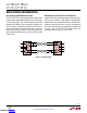
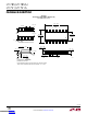
The high overvoltage rating of the LT1785/LT1791 facili
-
tates easy extension to almost any level. Simple discrete
component
networks
that limit the receiver input and
driver output voltages to less than ±60V can be added
to the device to extend protection to any desired level.
Figure 11 shows a protection network against faults to
the120VAC line voltage.
The LT1785/LT1791 protection is achieved by using a high
voltage bipolar integrated circuit process for the transceiv
-
ers. The naturally high breakdown voltages of the bipolar
process provides protection in powered-off and high
impedance
conditions.
The driver outputs use a foldback
current limit design to protect against overvoltage faults
while still allowing high current output drive.
ESD Protection
The LT1785/LT1791 I/O pins have on-chip ESD protection
circuitry to eliminate field failures caused by discharges to
exposed ports and cables in application environments. The
LT1785 pins A and B and the LT1791 driver output pins Y
and Z are protected to IEC-1000-4-2 level 2. These pins will
survive multiple ESD strikes of ±15kV air discharge or ±4kV
contact discharge. Due to their very high input impedance,
the LT1791 receiver pins are protected to IEC-1000-4-2
level 2, or ±15kV air and ±4kV contact discharges. This
level of ESD protection will guarantee immunity from field
failures in all but the most severe ESD environments. The
LT1791 receiver input ESD tolerance may be increased to
IEC level 4 compliance by adding 2.2k resistors in series
with these pins.
Low Power Shutdown
The LT1785/LT1791 have RE and DE logic inputs to control
the receive and transmit modes of the transceivers. The
RE input allows normal data reception when in the low
state. The receiver output goes to a high impedance state
when RE is high, allowing multiplexing the RO data line.
The DE logic input performs a similar function on the driver
outputs. A high state on DE activates the differential driver
outputs, a low state places both driver outputs in to high
impedance. Tying the RE and DE logic inputs together may
be done to allow one logic signal to toggle the transceiver
from receive to transmit modes. The DE input is used as
the data input in CAN bus applications.
Disabling both the driver and receiver places the device
into a low supply current shutdown mode. An internal
time delay of 3µs minimum prevents entering shutdown
due to small logic skews when a toggle between receive
and transmit is desired. The recovery time from shutdown
mode is typically 12µs. The user must be careful to allow
for this wake-up delay from shutdown mode. To allow full
250kbaud data rate transmission in CAN applications, the
RE pin should be tied low to prevent entering shutdown
mode.
Downloaded from Arrow.com.Downloaded from Arrow.com.Downloaded from Arrow.com.Downloaded from Arrow.com.Downloaded from Arrow.com.Downloaded from Arrow.com.Downloaded from Arrow.com.Downloaded from Arrow.com.Downloaded from Arrow.com.Downloaded from Arrow.com.Downloaded from Arrow.com.