
Datasheet


10
LT1792
U
S
A
O
PP
L
IC
AT
I
WU
U
I FOR ATIO
also increases the parasitic gate capacitance, which if left
unchecked, can result in increased overshoot and ring-
ing. When the feedback around the op amp is resistive
(R
F
), a pole will be created with R
F
, the source resistance
and capacitance (R
S
, C
S
), and the amplifier input capaci-
tance (C
IN
= 27pF). In low gain configurations and with
R
S
and R
F
in the kilohm range (Figure 5), this pole can
create excess phase shift and even oscillation. A small
capacitor (C
F
) in parallel with R
F
eliminates this problem.
With R
S
(C
S
+ C
IN
) = R
F
C
F
, the effect of the feedback pole
is completely removed.
Figure 5
–
+
1792 F05
OUTPUT
R
F
R
S
C
S
C
F
C
IN
1792 TA06
V
OUT
TYPICAL OFFSET ≈ 0.8mV
1% TOLERANCES
FOR V
IN
= 10V
P-P
, V
OUT
= –121dB AT f > 330Hz
= – 6dB AT f = 16.3Hz
LOWER RESISTOR VALUES WILL RESULT IN LOWER THERMAL NOISE AND LARGER CAPACITORS
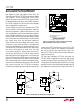
R3
249k
C2
100nF
C1
33nF
R1
237k
V
IN
R2
237k
R6
249k
C4
330nF
3
2
–
+
LT1792
6
C3
10nF
R4
154k
R5
154k
7
15V
–15V
4
6
3
2
–
+
LT1792
10Hz Fourth Order Chebyshev Lowpass Filter (0.01dB Ripple)
U
SA
O
PP
L
IC
AT
ITY
P
I
CA
L
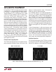
Accelerometer Amplifier with DC Servo
7
5V TO 15V
–5V TO –15V
4
1792 TA03
OUTPUT
R1
100M
C1
1250pF
R3
2k
C3
2µF
R2
18k
C2
2µF
2
3
R4
20M
–
+
LT1792
6
R5
20M
ACCELEROMETER
B & K MODEL 4381
OR EQUIVALENT
6
3
2
–
+
LT1792
R4C2 = R5C3 > R1 (1 + R2/R3) C1
OUTPUT = 0.8mV/pC* = 8.0mV/g**
DC OUTPUT ≤ 2.7mV
OUTPUT NOISE = 6nV/√Hz AT 1kHz
*PICOCOULOMBS
**g = EARTH’S GRAVITATIONAL CONSTANT