
Datasheet


7
LT1792
CCHARA TERIST
ICS
UW
AT
Y
P
I
CA
LPER
F
O
R
C
E
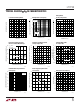
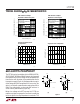
THD and Noise vs Output
Amplitude for Noninverting Gain
OUTPUT SWING (V
P-P
)
0.001
TOTAL HARMONIC DISTORTION + NOISE (%)
0.01
0.1
1
11030
1792 G18
0.0001
0.3
Z
L
= 2k 15pF, f
O
= 1kHz
A
V
= 1, 10, 100
MEASUREMENT BANDWIDTH
= 10Hz TO 22kHz
A
V
= 100
A
V
= 10
A
V
= 1
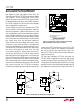
THD and Noise vs Output
Amplitude for Inverting Gain
OUTPUT SWING (V
P-P
)
0.001
TOTAL HARMONIC DISTORTION + NOISE (%)
0.01
0.1
1
11030
1792 G19
0.0001
0.3
Z
L
= 2k 15pF, f
O
= 1kHz
A
V
= –1, –10, –100
MEASUREMENT BANDWIDTH
= 10Hz TO 22kHz
A
V
= –100
A
V
= –10
A
V
= –1
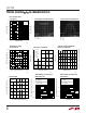
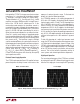
TEMPERATURE (°C)
–75
10
OUTPUT CURRENT (mA)
15
20
25
30
–25 5025
100
1792 G20
35
40
–50 0
75
125
SINK SOURCE
V
S
= ±15V
Short-Circuit Output Current
vs Temperature
TEMPERATURE (°C)
–75
3
SUPPLY CURRENT (mA)
4
–25 5025
100
1792 G21
5
–50 0
75
125
V
S
= ±15V
V
S
= ±5V
Supply Current vs Temperature
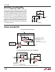
Figure 1
2
3
1
5
∆V
OS
= ±10mV
50k
15V
–15V
1792 F01a
4
6
7
–
+
2
3
1
5
∆V
OS
= ±1mV
50k
10k
10k
15V
–15V
1792 F01b
4
6
7
–
+
(b)(a)
U
S
A
O
PP
L
IC
AT
I
WU
U
I FOR ATIO
The LT1792 may be inserted directly into OPA124, AD743,
AD745, AD645, AD544 and AD820 sockets with improved
noise performance. Offset nulling will be compatible with
these devices with the wiper of the potentiometer tied to
the negative supply (Figure 1a). No appreciable change in
offset voltage drift with temperature will occur when the
device is nulled with a potentiometer ranging from 10k to
200k. Finer adjustments can be made with resistors in
series with the potentiometer (Figure 1b).
Being a low voltage noise JFET op amp, the LT1792 can
replace many bipolar op amps that are used in amplifying
low level signals from high impedance transducers. The