
Datasheet


8
LT1792
U
S
A
O
PP
L
IC
AT
I
WU
U
I FOR ATIO
best bipolar op amps, with higher current noise, will
eventually lose out to the LT1792 when transducer imped-
ance increases. The low voltage noise of the LT1792
allows it to surpass most single JFET op amps available.
For the best performance versus area available anywhere,
the LT1792 is offered in the SO-8 surface mount package
with no degradation in performance.
The low voltage and current noise offered by the LT1792
makes it useful in a wide range of applications, especially
where high impedance, capacitive transducers are used
such as hydrophones, precision accelerometers and photo
diodes. The total output noise in such a system is the gain
times the RMS sum of the op amp input referred voltage
noise, the thermal noise of the transducer, and the op amp
bias current noise times the transducer impedance.
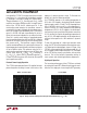
Figure 2 shows total input voltage noise versus source
resistance. In a low source resistance (<5k) application
the op amp voltage noise will dominate the total noise.
This means the LT1792 will beat out any JFET op amp, only
the lowest noise bipolar op amps have the edge
at low source resistances. As the source resistance in-
creases from 5k to 50k, the LT1792 will match the best
bipolar op amps for noise performance, since the thermal
noise of the transducer (4kTR) begins to dominate the
total noise. A further increase in source resistance, above
50k, is where the op amp’s current noise component (2qI
B
R
TRANS
) will eventually dominate the total noise. At these
high source resistances, the LT1792 will out perform
the lowest noise bipolar op amp due to the inherently low
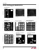
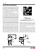
Figure 3. Noninverting and Inverting Gain Configurations
–
+
R2
OUTPUT
R
B
C
B
R1
C
S
R
S
C
B
≅ C
S
R
B
= R
S
R
S
> R1
OR R2
TRANSDUCER
–
+
OUTPUT
C
F
C
B
R
B
C
B
= C
F
C
S
R
B
= R
F
R
S
R
F
C
S
R
S
TRANSDUCER
1792 F03
Q = CV; = I = C
dQ
dt
dV
dt
SOURCE RESISTANCE (Ω)
100
1
10
1k
1k 100M
1792 F02
100k
100
10M10k 1M
RESISTOR NOISE ONLY
INPUT NOISE VOLTAGE (nV/
√
H
z)
V
n
= A
V
√V
n
2
(OP AMP)
+ 4kTR
+ 2
q
I
B
• R
2
+
–
C
S
R
S
V
O
C
S
R
S
LT1007
LT1792
LT1007*
LT1792*
SOURCE RESISTANCE = 2R
S
= R
* PLUS RESISTOR
†
PLUS RESISTOR 1000pF CAPACITOR
LT1792
†
LT1007
†
Figure 2. Comparison of LT1792 and LT1007 Total Output
1kHz Voltage Noise Versus Source Resistance
current noise of FET input op amps. Clearly, the LT1792
will extend the range of high impedance transducers
that can be used for high signal-to-noise ratios. This
makes the LT1792 the best choice for high impedance,
capacitive transducers.
The high input impedance JFET front end makes the
LT1792 suitable in applications where very high charge
sensitivity is required. Figure 3 illustrates the LT1792 in its
inverting and noninverting modes of operation. A charge
amplifier is shown in the inverting mode example; here the
gain depends on the principal of charge conservation at