
Datasheet


9
LT1792
U
S
A
O
PP
L
IC
AT
I
WU
U
I FOR ATIO
the input of the LT1792. The charge across the transducer
capacitance, C
S
, is transferred to the feedback capacitor
C
F
, resulting in a change in voltage, dV, equal to dQ/C
F
.
The gain therefore is C
F
/C
S
. For unity gain, the C
F
should
equal the transducer capacitance plus the input capaci-
tance of the LT1792 and R
F
should equal R
S
. In the
noninverting mode example, the transducer current is
converted to a change in voltage by the transducer capaci-
tance; this voltage is then buffered by the LT1792 with a
gain of 1 + R1/R2. A DC path is provided by R
S
, which is
either the transducer impedance or an external resistor.
Since R
S
is usually several orders of magnitude greater
than the parallel combination of R1 and R2, R
B
is added to
balance the DC offset caused by the noninverting input
bias current and R
S
. The input bias currents, although
small at room temperature, can create significant errors at
higher temperature, especially with transducer resistances
of up to 100M or more. The optimum value for R
S
is
determined by equating the thermal noise (4kTR
S
) to the
current noise times R
S
, [(2qI
B
) • R
S
], resulting in
R
B
= 2V
T
/I
B
(V
T
= 26mV at 25°C). A parallel capacitor, C
B
,
is used to cancel the phase shift caused by the op amp
input capacitance and R
B
.
Reduced Power Supply Operation
The LT1792 can be operated from ±5V supplies for lower
power dissipation resulting in lower I
B
and noise at the
expense of reduced dynamic range. To illustrate this
benefit, let’s take the following example:
An LT1792CS8 operates at an ambient temperature of
25°C with ±15V supplies, dissipating 159mW of power
(typical supply current = 5.3mA). The SO-8 package has a
θ
JA
of 190°C/W, which results in a die temperature in-
crease of 30.2°C or a room temperature die operating
temperature of 55.2°C. At ±5V supplies, the die tempera-
ture increases by only one third of the previous amount or
10.1°C resulting in a typical die operating temperature of
only 35.1°C. A 20 degree reduction of die temperature is
achieved at the expense of a 20V reduction in dynamic
range.
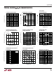
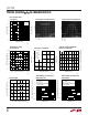
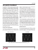
To take full advantage of a wide input common mode
range, the LT1792 was designed to eliminate phase rever-
sal. Referring to the photographs shown in Figure 4, the
LT1792 is shown operating in the follower mode (A
V
= 1)
at ±5V supplies with the input swinging ±5.2V. The output
of the LT1792 clips cleanly and recovers with no phase
reversal. This has the benefit of preventing lock-up in
servo systems and minimizing distortion components.
High Speed Operation
The low noise performance of the LT1792 was achieved
by making the input JFET differential pair large to maxi-
mize the first stage gain. Increasing the JFET geometry
INPUT: ±5.2V Sine Wave LT1792 Output
1792 F04a 1792 F03b
Figure 4. Voltage Follower with Input Exceeding the Common Mode Range ( V
S
= ±5V)