
Datasheet

2
LT1794
ORDER PART
NUMBER
Supply Voltage (V
+
to V
–
) .................................... ±18V
Input Current ..................................................... ±10mA
Output Short-Circuit Duration (Note 2)........... Indefinite
Operating Temperature Range ............... –40°C to 85°C
LT1794CFE
LT1794IFE
T
JMAX
= 150°C, θ
JA
= 40°C/W, θ
JC
= 3°C/W (Note 4)
Consult factory for parts specified with wider operating temperature ranges.
ABSOLUTE MAXIMUM RATINGS
W
WW
U
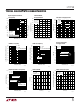
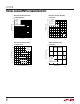
PACKAGE/ORDER INFORMATION
W
U
U
Specified Temperature Range (Note 3).. –40°C to 85°C
Junction Temperature.......................................... 150°C
Storage Temperature Range ................. –65°C to 150°C
Lead Temperature (Soldering, 10 sec).................. 300°C
(Note 1)
ORDER PART
NUMBER
LT1794CSW
LT1794ISW
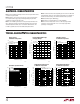
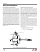
1
2
3
4
5
6
7
8
9
10
TOP VIEW
SW PACKAGE
20-LEAD PLASTIC SO
20
19
18
17
16
15
14
13
12
11
NC
V
+
OUT
V
–
V
–
V
–
V
–
–IN
+IN
SHDN
NC
V
+
OUT
V
–
V
–
V
–
V
–
–IN
+IN
SHDNREF
1
2
3
4
5
6
7
8
9
10
TOP VIEW
20
19
18
17
16
15
14
13
12
11
V
–
NC
–IN
+IN
SHDN
SHDNREF
+IN
–IN
NC
V
–
V
–
NC
OUT
V
+
NC
NC
V
+
OUT
NC
V
–
FE PACKAGE
20-LEAD PLASTIC TSSOP
T
JMAX
= 150°C, θ
JA
= 40°C/W, θ
JC
= 3°C/W (Note 4)
UNDERSIDE METAL CONNECTED TO V
–
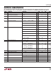
ELECTRICAL CHARACTERISTICS
The ● denotes the specifications which apply over the full specified temperature range, otherwise specifications are at T
A
= 25°C.
V
CM
= 0V, pulse tested, ±5V ≤ V
S
≤ ±15V, V
SHDNREF
= 0V, R
BIAS
= 24.9k between V
+
and SHDN unless otherwise noted. (Note 3)
SYMBOL PARAMETER CONDITIONS MIN TYP MAX UNITS
V
OS
Input Offset Voltage 15.0 mV
● 7.5 mV
Input Offset Voltage Matching 0.3 5.0 mV
● 7.5 mV
Input Offset Voltage Drift ● 10 µV/°C
I
OS
Input Offset Current 100 500 nA
● 800 nA
I
B
Input Bias Current ±0.1 ±4 µA
● ±6 µA
Input Bias Current Matching 100 500 nA
● 800 nA
e
n
Input Noise Voltage Density f = 10kHz 8 nV/√Hz
i
n
Input Noise Current Density f = 10kHz 0.8 pA/√Hz
R
IN
Input Resistance V
CM
= (V
+
– 2V) to (V
–
+ 2V) ● 550 MΩ
Differential 6.5 MΩ