
Datasheet

4
LT1794
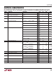
ELECTRICAL CHARACTERISTICS
Note 1: Absolute Maximum Ratings are those values beyond which the life
of a device may be impaired.
Note 2: Applies to short circuits to ground only. A short circuit between
the output and either supply may permanently damage the part when
operated on supplies greater than ±10V.
Note 3: The LT1794C is guaranteed to meet specified performance from
0°C to 70°C and is designed, characterized and expected to meet these
extended temperature limits, but is not tested at –40°C and 85°C. The
LT1794I is guaranteed to meet the extended temperature limits.
Note 4: Thermal resistance varies depending upon the amount of PC board
metal attached to the device. If the maximum dissipation of the package is
exceeded, the device will go into thermal shutdown and be protected.
Note 5: Guaranteed by the CMRR tests.
Note 6: R
BIAS
is connected between V
+
and the SHDN pin.
Note 7: Slew rate is measured at ±5V on a ±10V output signal while
operating on ±15V supplies and ±1V on a ±3V output signal while
operating on ±5V supplies.
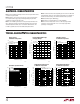
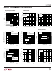
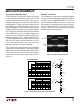
TYPICAL PERFOR A CE CHARACTERISTICS
UW
Supply Current
vs Ambient Temperature
Input Common Mode Range
vs Supply Voltage
Input Bias Current
vs Ambient Temperature
SUPPLY VOLTAGE (±V)
2
V
–
COMMON MODE RANGE (V)
1.0
2.0
–2.0
4
6
810
1794 G02
12
–1.0
V
+
0.5
1.5
–1.5
–0.5
14
T
A
= 25°C
∆V
OS
> 1mV
TEMPERATURE (
°C)
–50
I
SUPPLY
PER AMPLIFIER (mA)
11
13
15
1794 G01
9
7
10
12
14
8
6
5
–30 –10 10 30 50 70 90
V
S
= ±12V
R
BIAS
= 24.9k TO SHDN
V
SHDNREF
= 0V
TEMPERATURE (°C)
–50
±I
BIAS
(nA)
120
160
200
50
1794 G03
80
40
100
140
180
60
20
0
–30
–10
10 30
70 90
V
S
= ±12V
I
S
PER AMPLIFIER = 10mA
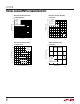
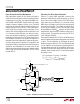
Input Noise Spectral Density
Output Short-Circuit Current
vs Ambient Temperature
Output Saturation Voltage
vs Ambient Temperature
FREQUENCY (Hz)
1
INPUT VOLTAGE NOISE (V/VHz)
INPUT CURRENT NOISE (pA/VHz)
10
1 100 1k 10k
1794 G04
0.1
10
100
1
10
0.1
100
100k
e
n
i
n
T
A
= 25°C
V
S
= ±12V
I
S
PER AMPLIFIER = 10mA
TEMPERATURE (°C)
–50
600
I
SC
(mA)
620
660
680
700
800
740
–10
30
50
1794 G05
640
760
780
720
–30 10
70
90
V
S
= ±12V
I
S
PER AMPLIFIER = 10mA
SINKING
SOURCING
TEMPERATURE (°C)
–50
OUTPUT SATURATION VOLTAGE (V)
–0.5
10
1794 G06
1.0
–30 –10 30
0.5
V
–
V
+
–1.0
–1.5
1.5
50 70 90
V
S
= ±12V
R
L
= 100Ω
R
L
= 100Ω
I
LOAD
= 250mA
I
LOAD
= 250mA