
Datasheet

7
LT1794
9
2
8
–12V
1k
12V
3
19
10 (SHDN)
R
SHDN
4
5
6
7
110Ω
OUT (+)
OUT (–)
10k
E
IN
0.01µF
R
L
≈ 50Ω
1:2*
10k
49.9Ω
110Ω
12.7Ω
1794 TC
14
15
16
17
18
11 (SHDNREF)
–
+
A
13
12
1k
0.1µF 4.7µF
0.1µF
12V
–12V
–
+
B
–12V
12.7Ω
V
OUT(P-P)
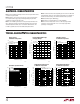
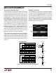
100 LINE LOAD
SUPPLY BYPASSING
*COILCRAFT X8390-A OR EQUIVALENT
V
OUTP-P
AMPLITUDE SET AT EACH AMPLIFIER OUTPUT
DISTORTION MEASURED ACROSS LINE LOAD
SPLITTER
MINICIRCUITS
ZSC5-2-2
+
+
4.7µF
+
0.1µF
4.7µF
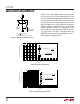
TEST CIRCUIT
APPLICATIO S I FOR ATIO
WUUU
The LT1794 is a high speed, 200MHz gain bandwidth
product, dual voltage feedback amplifier with high output
current drive capability, 500mA source and sink. The
LT1794 is ideal for use as a line driver in xDSL data
communication applications. The output voltage swing
has been optimized to provide sufficient headroom when
operating from ±12V power supplies in full-rate ADSL
applications. The LT1794 also allows for an adjustment of
the operating current to minimize power consumption. In
addition, the LT1794 is available in small footprint surface
mount packages to minimize PCB area in multiport central
office DSL cards.
To minimize signal distortion, the LT1794 amplifiers are
decompensated to provide very high open-loop gain at
high frequency. As a result each amplifier is frequency
stable with a closed-loop gain of 10 or more. If a closed-
loop gain of less than 10 is desired, external frequency
compensating components can be used.
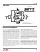
Setting the Quiescent Operating Current
Power consumption and dissipation are critical concerns
in multiport xDSL applications. Two pins, Shutdown
(SHDN) and Shutdown Reference (SHDNREF), are pro-
vided to control quiescent power consumption and allow
for the complete shutdown of the driver. The quiescent
current should be set high enough to prevent distortion
induced errors in a particular application, but not so high
that power is wasted in the driver unnecessarily. A good
starting point to evaluate the LT1794 is to set the quiescent
current to 10mA per amplifier.
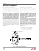
The internal biasing circuitry is shown in Figure 1. Ground-
ing the SHDNREF pin and directly driving the SHDN pin with
a voltage can control the operating current as seen in the
Typical Performance Characteristics. When the SHDN pin
is less than SHDNREF + 0.4V, the driver is shut down and
consumes typically only 100µA of supply current and the