
Datasheet


LT1806/LT1807
17
18067fc
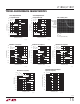
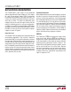
Rail-to-Rail Characteristics
The LT1806/LT1807 have input and output signal range that
covers from negative power supply to positive power sup-
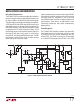
ply. Figure 1 depicts a simplifi ed schematic of the amplifi er.
The input stage is comprised of two differential amplifi ers,
a PNP stage Q1/Q2 and a NPN stage Q3/Q4 that are active
over different ranges of common mode input voltage. The
PNP differential pair is active between the negative supply
to approximately 1.5V below the positive supply. As the
input voltage moves closer toward the positive supply, the
transistor Q5 will steer the tail current I
1
to the current
mirror Q6/Q7, activating the NPN differential pair. The PNP
pair becomes inactive for the rest of the input common
mode range up to the positive supply.
APPLICATIONS INFORMATION
A pair of complementary common emitter stages Q14/Q15
that enable the output to swing from rail to rail constructs
the output stage. The capacitors C1 and C2 form the
local feedback loops that lower the output impedance at
high frequency. These devices are fabricated on Linear
Technology’s proprietary high speed complementary
bipolar process.
Power Dissipation
The LT1806/LT1807 amplifi ers combine high speed with
large output current in a small package, so there is a need
to ensure that the die’s junction temperature does not
exceed 150°C. The LT1806 is housed in an SO-8 package
or a 6-lead SOT-23 package and the LT1807 is in an SO-8
Q4
Q6
Q3
Q7
Q10
Q1
Q13 Q15
OUT
Q2
Q11
Q12
Q9
Q5 V
BIAS
I
1
D2
D1
D5
D4
D3
D6
D7
D8
ESDD2ESDD1
+IN
–IN
V
–
ESDD3ESDD4
V
+
V
+
V
–
Q8
R2R1
R3 R4 R5
Q14
18067 F01
+
I
2
C2
C
C
V
–
+
C1
BUFFER
AND
OUTPUT BIAS
Q17
Q16
ESDD5
SHDN
V
+
V
–
R7
100k
R6
40k
D9
V
+
V
–
ESDD6
BIAS
GENERATION
Figure 1. LT1806 Simplifi ed Schematic Diagram