
Datasheet


LT1910
5
1910fa
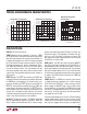
TYPICAL PERFORMANCE CHARACTERISTICS
Turn-On Time vs Temperature Turn-Off Time vs Temperature
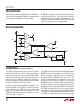
Automatic Restart Period
vs Temperature
TEMPERATURE (oC)
–50
TURN-ON TIME (Ms)
150
200
250
300
400
–25
02550
1910 G13
75 125100
350
100
V
+
= 24V
V
GATE
= 32V
C
GATE
= 1nF
TEMPERATURE (oC)
–50
0
TURN-OFF TIME (Ms)
20
40
60
50
–25
0
25 50
1910 G014
75
80
100
10
30
70
90
125100
V
+
= 24V
V
GATE
= 2V
C
GATE
= 1nF
NORMAL
CURRENT LIMIT
TEMPERATURE (°C)
–30
10
100
1000
–10 10 30 50
9070
1910 G15
AUTOMATIC RESTART PERIOD (ms)
–50
130110
V
+
= 24V
C
T
= 3.3μF
C
T
= 0.33μF
C
T
= 0.1μF
C
T
= 1μF
PIN FUNCTIONS
GND (Pin 1): Common Ground.
TIMER (Pin 2): A timing capacitor, C
T
, from the TIMER
pin to ground sets the restart time following overcurrent
detection. Upon detection of an overcurrent condition, C
T
is rapidly discharged to less than 1V and then recharged
by a 14μA nominal current source back to the 2.9V timer
threshold, whereupon the restart is attempted. When-
ever TIMER pulls below 2.9V, the GATE pin pulls low to
turn off the external switch. This cycle repeats until the
overcurrent condition goes away and the switch restarts
successfully. During normal operation the pin clamps at
3.5V nominal.
FAULT (Pin 3): The FAULT pin monitors the TIMER pin
voltage and indicates the overcurrent condition. Whenever
the TIMER pin is pulled below 3.3V at the onset of a cur-
rent limit condition, the FAULT pin pulls active LOW. The
FAULT pin resets HIGH immediately when the TIMER pin
ramps above 3.4V during autorestart. The FAULT pin is an
open-collector output, thus requiring an external pull-up
resistor and is intended for logic interface. The resistor
should be selected with a typical 1mA pull-up at low status
and less than 2mA under worst-case conditions.
IN (Pin 4): The IN pin threshold is TTL/CMOS compatible
and has approximately 200mV of hysteresis. When the
IN pin is pulled active HIGH above 2V, an internal charge
pump is activated to pull up the GATE pin. The IN pin can
be pulled as high as 15V regardless of whether the sup-
ply is on or off. If the IN pin is left open, an internal 75k
pull-down resistor pulls the pin below 0.8V to ensure that
the GATE pin is inactive LOW.
GATE (Pin 5): The GATE pin drives the power MOSFET
gate. When the IN pin is greater than 2V, the GATE pin is
pumped approximately 12V above the supply. It has rela-
tively high impedance (the equivalence of a few hundred
kΩ) when pumped above the rail. Care should be taken
to minimize any loading by parasitic resistance to ground
or supply. The GATE pin pulls LOW when the TIMER pin
falls below 2.9V.
SENSE (Pin 6): The SENSE pin connects to the input of
a supply-referenced comparator with a 65mV nominal
offset. When the SENSE pin is taken more than 65mV
below supply, the MOSFET gate is driven LOW and the
timing capacitor is discharged. The SENSE pin threshold
has a 0.33%/°C temperature coeffi cient (TC), which closely
matches the TC of the drain-sense resistor formed from
the copper trace of the PCB.
For loads requiring high inrush current, an RC timing delay
can be added between the drain-sense resistor and the
SENSE pin to ensure that the current-sense comparator
does not false trigger during start-up (see Applications