
Datasheet


LT1934/LT1934-1
7
1934fe
OPERATION
The LT1934 uses Burst Mode control, combining both low
quiescent current operation and high switching frequency,
which result in high effi ciency across a wide range of load
currents and a small total circuit size.
A comparator monitors the voltage at the FB pin of the
LT1934. If this voltage is higher than the internal 1.25V
reference, the comparator disables the oscillator and power
switch. In this state, only the comparator, reference and
undervoltage lockout circuits are active, and the current into
the V
IN
pin is just 12μA. As the load current discharges the
output capacitor, the voltage at the FB pin falls below 1.25V
and the comparator enables the oscillator. The LT1934
begins to switch, delivering current to the output capaci-
tor. The output voltage rises, and when it overcomes the
feedback comparator’s hysteresis, the oscillator is disabled
and the LT1934 returns to its micropower state.
The oscillator consists of two one-shots and a fl ip-fl op.
A rising edge from the off-time one-shot sets the fl ip-fl op,
which turns on the internal NPN power switch. The switch
remains on until either the on-time one-shot trips or the
current limit is reached. A sense resistor and amplifi er
monitor the current through the switch and resets the
(Refer to Block Diagram)
fl ip-fl op when this current reaches 400mA (120mA for
the LT1934-1). After the 1.8μs delay of the off-time one-
shot, the cycle repeats. Generally, the LT1934 will reach
current limit on every cycle—the off time is fi xed and
the on time is regulated so that the LT1934 operates at
the correct duty cycle. The 1.8μs off time is lengthened
when the FB pin voltage falls below 0.8V; this foldback
behavior helps control the output current during start-up
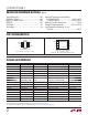
and overload. Figure 1 shows several waveforms of an
LT1934 producing 3.3V from a 10V input. When the switch
is on, the SW pin voltage is at 10V. When the switch is
off, the inductor current pulls the SW pin down until it is
clamped near ground by the external catch diode.
The switch driver operates from either the input or from
the BOOST pin. An external capacitor and diode are used
to generate a voltage at the BOOST pin that is higher than
the input supply. This allows the driver to fully saturate
the bipolar switch for effi cient operation.
If the SHDN pin is grounded, all internal circuits are turned
off and V
IN
current reduces to the device leakage current,
typically a few nA.
V
OUT
50mV/DIV
V
SW
10V/DIV
Figure 1. Operating Waveforms of the LT1934 Converting
10V to 3.3V at 180mA (Front Page Schematic)
1934 F01a
I
SW
0.5A/DIV
I
LI
0.5A/DIV
5μs/DIV