
Datasheet


LT1941
19
1941fb
APPLICATIONS INFORMATION
THERMAL CONSIDERATIONS
The PCB must provide heat sinking to keep the LT1941
cool. The Exposed Pad on the bottom of the package must
be soldered to a ground plane. This ground should be tied
to other copper layers below with thermal vias; these lay-
ers will spread the heat dissipated by the LT1941. Place
additional vias near the catch diodes. Adding more copper
to the top and bottom layers and tying this copper to the
internal planes with vias can reduce thermal resistance
further. With these steps, the thermal resistance from die
(or junction) to ambient can be reduced to θ
JA
= 25°C/W
or less. With 100 LFPM airfl ow, this resistance can fall
by another 25%. Further increases in airfl ow will lead to
lower thermal resistance.
Because of the large output current capability of the LT1941,
it is possible to dissipate enough heat to raise the junction
temperature beyond the absolute maximum of 125°C. If
two of the channels are running at full output current, the
third channel may have reduced output current capability,
limited by the maximum junction temperature. The output
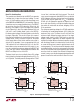
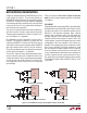
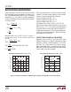
Figure 7. Subtracting the Current when the Switch is ON (a) From the Current when the Switch is OFF (b) Reveals the Path
of the High Frequency Switching Current (c) Keep This Loop Small. The Voltage on the SW and BOOST Nodes will also be
Switched; Keep these Nodes as Small as Possible. Finally, Make Sure the Circuit is Shielded with a Local Ground Plane
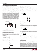
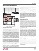
Figure 8. Power Path Components and Topside Layout
V
IN
SW
GND
(a)
V
IN
V
SW
C1 D1 C2
1941 F07
L1
SW
GND
(c)
V
IN
SW
GND
(b)
I
C1
GND
GND
GND
V
OUT1
V
IN
C
IN1
C
IN2
L3 L4
L1
1941 F08
C7
C12
C10
C11
D1
C8
D3
PLACE VIAS UNDER GROUND PAD
TO GROUND PLANE FOR GOOD
THERMAL CONDUCTIVITY
D4
D5
D2
U1
V
OUT2
V
OUT3
GND
C9