
Datasheet


LT1963A Series
18
1963aff
For more information www.linear.com/LT1963A
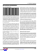
applicaTions inForMaTion
typically 40nV/√Hz over this frequency bandwidth for
the LT1963A (adjustable version). For higher output
voltages (generated by using a resistor divider), the
output voltage noise will be gained up accordingly. This
results in RMS noise over the 10Hz to 100kHz bandwidth
of 14µV
RMS
for the LT1963A increasing to 38µV
RMS
for
the LT1963A-3.3.
Higher values of output voltage noise may be measured
when care is not exercised with regard to circuit layout
and testing. Crosstalk from nearby traces can induce
unwanted
noise onto the output of the LT1963A-X.
Power supply ripple rejection must also be considered; the
LT1963A regulators do not have unlimited power supply
rejection and will pass a small portion of the input noise
through to the output.
Thermal Considerations
The power handling capability of the device is limited by the
maximum rated junction temperature (125°C). The power
dissipated by the device is made up of two components:
1. Output current multiplied by the input/output voltage
differential: (I
OUT
)(V
IN
– V
OUT
), and
2. GND pin current multiplied by the input voltage: (I
GND
)
(V
IN
).
The GND pin current can be found using the GND Pin
Current curves in
the Typical Per
formance Characteristics.
Power dissipation will be equal to the sum of the two
components listed above.
The LT1963A series regulators have internal thermal
limiting designed to protect the device during overload
conditions. For continuous normal conditions, the maxi
-
mum junction temperature rating of 125°C must not be
exceeded. It is important to give careful consideration to
all
sources of thermal resistance from junction to ambi-
ent. Additional
heat sources mounted nearby must also
be considered.
For surface mount devices, heat sinking is accomplished
by using the heat spreading capabilities of the PC board
and its copper traces. Copper board stiffeners and plated
through-holes can also be used to spread the heat gener
-
ated by power devices.
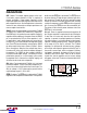
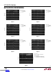
This
resistor should be made using one of the inner
layers of the PC board which are well defined. The resistiv-
ity is determined primarily by the sheet resistance of the
copper laminate with no additional plating steps. Table
2 gives some sizes for 0.75A RMS current for various
copper thicknesses. More detailed information regarding
resistors made from PC traces can be found in Application
Note 69, Appendix A.
Overload Recovery
Like many IC power regulators, the LT1963A-X has safe op-
erating area protection. The safe area protection decreases
the current limit as input-to-output voltage increases and
keeps the power transistor inside a safe operating region
for all values of input-to-output voltage. The protection
is designed to provide some output current at all values
of input-to-output voltage up to the device breakdown.
When power is first turned on, as the input voltage rises,
the output follows the input, allowing the regulator to start
up into very heavy loads. During the start-up, as the input
voltage is rising, the input-to-output voltage differential
is small, allowing the regulator to supply large output
currents. With a high input voltage, a problem can occur
wherein removal of an output short will not allow the
output voltage to recover. Other regulators, such as the
LT1085, also exhibit this phenomenon, so it is not unique
to the LT1963A-X.
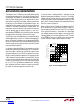
The problem occurs with a heavy output load when the
input voltage is high and the output voltage is low. Common
situations are immediately after the removal of a short-
circuit or when the shutdown pin is pulled high after the
input voltage has already
been turned on. The load line for
such a load may intersect the output current curve at two
points. If this happens, there are two stable output operat
-
ing points for the regulator. With this double intersection,
the input power supply may need to be cycled down to
zero and brought up again to make the output recover.
Output Voltage Noise
The LT1963A regulators have been designed to provide
low output voltage noise over the 10Hz to 100kHz band
-
width while operating at full load. Output voltage noise is
Downloaded from Arrow.com.Downloaded from Arrow.com.Downloaded from Arrow.com.Downloaded from Arrow.com.Downloaded from Arrow.com.Downloaded from Arrow.com.Downloaded from Arrow.com.Downloaded from Arrow.com.Downloaded from Arrow.com.Downloaded from Arrow.com.Downloaded from Arrow.com.Downloaded from Arrow.com.Downloaded from Arrow.com.Downloaded from Arrow.com.Downloaded from Arrow.com.Downloaded from Arrow.com.Downloaded from Arrow.com.Downloaded from Arrow.com.