
Datasheet


14
LT1963 Series
1963fc
device. If the input is left open circuit or grounded, the ADJ
pin will act like an open circuit when pulled below ground
and like a large resistor (typically 5k) in series with a diode
when pulled above ground.
In situations where the ADJ pin is connected to a resistor
divider that would pull the ADJ pin above its 7V clamp
voltage if the output is pulled high, the ADJ pin input
current must be limited to less than 5mA. For example, a
resistor divider is used to provide a regulated 1.5V output
from the 1.21V reference when the output is forced to 20V.
The top resistor of the resistor divider must be chosen to
limit the current into the ADJ pin to less than 5mA when the
ADJ pin is at 7V. The 13V difference between OUT and ADJ
pins divided by the 5mA maximum current into the ADJ pin
yields a minimum top resistor value of 2.6k.
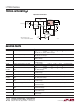
In circuits where a backup battery is required, several
different input/output conditions can occur. The output
voltage may be held up while the input is either pulled to
ground, pulled to some intermediate voltage, or is left
open circuit. Current flow back into the output will follow
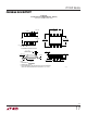
the curve shown in Figure 5.
When the IN pin of the LT1963 is forced below the OUT pin
or the OUT pin is pulled above the IN pin, input current will
typically drop to less than 2µA. This can happen if the
input of the device is connected to a discharged (low
voltage) battery and the output is held up by either a
backup battery or a second regulator circuit. The state of
the SHDN pin will have no effect on the reverse output
current when the output is pulled above the input.
Using a DD package, the thermal resistance will be in the
range of 23°C/W to 33°C/W depending on the copper
area. So the junction temperature rise above ambient will
be approximately equal to:
1.41W(28°C/W) = 39.5°C
The maximum junction temperature will then be equal to
the maximum junction temperature rise above ambient
plus the maximum ambient temperature or:
T
JMAX
= 50°C + 39.5°C = 89.5°C
Protection Features
The LT1963 regulators incorporate several protection
features which make them ideal for use in battery-powered
circuits. In addition to the normal protection features
associated with monolithic regulators, such as current
limiting and thermal limiting, the devices are protected
against reverse input voltages, reverse output voltages
and reverse voltages from output to input.
Current limit protection and thermal overload protection
are intended to protect the device against current overload
conditions at the output of the device. For normal opera-
tion, the junction temperature should not exceed 125°C.
The input of the device will withstand reverse voltages of
20V. Current flow into the device will be limited to less than
1mA (typically less than 100µA) and no negative voltage
will appear at the output. The device will protect both itself
and the load. This provides protection against batteries
that can be plugged in backward.
The output of the LT1963 can be pulled below ground
without damaging the device. If the input is left open circuit
or grounded, the output can be pulled below ground by
20V. For fixed voltage versions, the output will act like a
large resistor, typically 5k or higher, limiting current flow
to typically less than 600µA. For adjustable versions, the
output will act like an open circuit; no current will flow out
of the pin. If the input is powered by a voltage source, the
output will source the short-circuit current of the device
and will protect itself by thermal limiting. In this case,
grounding the SHDN pin will turn off the device and stop
the output from sourcing the short-circuit current.
The ADJ pin of the adjustable device can be pulled above
or below ground by as much as 7V without damaging the
APPLICATIO S I FOR ATIO
WUUU
Figure 5. Reverse Output Current
OUTPUT VOLTAGE (V)
0
REVERSE OUTPUT CURRENT (mA)
3.0
4.0
5.0
8
1963 F05
2.0
1.0
2.5
3.5
4.5
1.5
0.5
0
2
1
3
4
6
9
7
5
10
LT1963
V
OUT
= V
ADJ
T
J
= 25°C
V
IN
= 0V
CURRENT FLOWS
INTO OUTPUT PIN
LT1963-3.3
V
OUT
= V
FB
LT1963-1.5
V
OUT
= V
FB
LT1963-1.8
V
OUT
= V
FB
LT1963-2.5
V
OUT
= V
FB