
Datasheet


LT1964
11
1964fb
APPLICATIONS INFORMATION
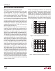
Figure 1. Adjustable Operation
The LT1964 is a 200mA negative low dropout regulator with
micropower quiescent current and shutdown. The device
is capable of supplying 200mA at a dropout voltage of
340mV. Output voltage noise can be lowered to 30μV
RMS
over a 10Hz to 100kHz bandwidth with the addition of a
0.01μF reference bypass capacitor. Additionally, the refer-
ence bypass capacitor will improve transient response of
the regulator, lowering the settling time for transient load
conditions. The low operating quiescent current (30μA)
drops to 3μA in shutdown. In addition to the low quies-
cent current, the LT1964 incorporates several protection
features which make it ideal for use in battery-powered
systems. In dual supply applications where the regulator
load is returned to a positive supply, the output can be
pulled above ground by as much as 20V and still allow
the device to start and operate.
Adjustable Operation
The adjustable version of the LT1964 has an output volt-
age range of –1.22V to –20V. The output voltage is set by
the ratio of two external resistors as shown in Figure 1.
The device servos the output to maintain the voltage at
the ADJ pin at –1.22V referenced to ground. The current
in R1 is then equal to –1.22V/R1 and the current in R2 is
the current in R1 plus the ADJ pin bias current. The ADJ
pin bias current, 30nA at 25°C, fl ows through R2 out of
the ADJ pin. The output voltage can be calculated using
the formula in Figure 1. The value of R1 should be less
than 250k to minimize errors in the output voltage caused
by the ADJ pin bias current. Note that in shutdown the
output is turned off and the divider current will be zero.
Curves of ADJ Pin Voltage vs Temperature and ADJ Pin Bias
Current vs Temperature appear in the Typical Performance
Characteristics section.
The adjustable device is tested and specifi ed with the ADJ
pin tied to the OUT pin and a 5μA DC load (unless otherwise
specifi ed) for an output voltage of –1.22V. Specifi cations
for output voltages greater than –1.22V will be propor-
tional to the ratio of the desired output voltage to –1.22V;
(V
OUT
/ –1.22V). For example, load regulation for an output
current change of 1mA to 200mA is 2mV typical at V
OUT
=
–1.22V. At V
OUT
= –12V, load regulation is:
(–12V/–1.22V) • (2mV) = 19.6mV
Bypass Capacitance and Low Noise Performance
The LT1964 may be used with the addition of a bypass
capacitor from V
OUT
to the BYP pin to lower output voltage
noise. A good quality low leakage capacitor is recom-
mended. This capacitor will bypass the reference of the
LT1964, providing a low frequency noise pole. The noise
pole provided by this bypass capacitor will lower the out-
put voltage noise to as low as 30μV
RMS
with the addition
of a 0.01μF bypass capacitor. Using a bypass capacitor
has the added benefi t of improving transient response.
With no bypass capacitor and a 10μF output capacitor, a
–10mA to –200mA load step will settle to within 1% of
its fi nal value in less than 100μs. With the addition of a
0.01μF bypass capacitor, the output will stay within 1%
for the same –10mA to –200mA load step (see LT1964-5
Transient Response in the Typical Characteristics section).
However, regulator start-up time is proportional to the size
of the bypass capacitor.
Higher values of output voltage noise may be measured
if care is not exercised with regard to circuit layout and
testing. Crosstalk from nearby traces can induce unwanted
noise onto the output of the LT1964-X.
1964 F01
GND
ADJ
IN
OUT
LT1964
V
IN
V
OUT
+
R1
R2
V
OUT
= –1.22V(1 + ) – (I
ADJ
)(R2)
V
ADJ
= –1.22V
I
ADJ
= 30nA AT 25°C
OUTPUT RANGE = –1.22V TO –20V
R2
R1