
Datasheet


LT1964
13
1964fb
APPLICATIONS INFORMATION
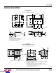
amounts of noise, especially when a ceramic capacitor is
used for noise bypassing. A ceramic capacitor produced
Figure 4’s trace in response to light tapping from a pencil.
Similar vibration induced behavior can masquerade as
increased output voltage noise.
For surface mount devices, heat sinking is accomplished
by using the heat spreading capabilities of the PC board
and its copper traces. Copper board stiffeners and plated
through-holes can also be used to spread the heat gener-
ated by power devices.
The following tables list thermal resistance for several
different board sizes and copper areas. All measurements
were taken in still air on 3/32" FR-4 board with one ounce
copper.
Table 1. SOT-23 Thermal Resistance
COPPER AREA
BOARD AREA
THERMAL RESISTANCE
(JUNCTION-TO-AMBIENT)TOPSIDE* BACKSIDE
2500mm
2
2500mm
2
2500mm
2
125°C/W
1000mm
2
2500mm
2
2500mm
2
125°C/W
225mm
2
2500mm
2
2500mm
2
130°C/W
100mm
2
2500mm
2
2500mm
2
135°C/W
50mm
2
2500mm
2
2500mm
2
150°C/W
*Device is mounted on topside.
Table 2. DFN Thermal Resistance
COPPER AREA
BOARD AREA
THERMAL RESISTANCE
(JUNCTION-TO-AMBIENT)TOPSIDE* BACKSIDE
2500mm
2
2500mm
2
2500mm
2
40°C/W
1000mm
2
2500mm
2
2500mm
2
45°C/W
225mm
2
2500mm
2
2500mm
2
50°C/W
100mm
2
2500mm
2
2500mm
2
62°C/W
*Device is mounted on topside.
The thermal resistance junction-to-case (θ
JC
), measured
at Pin 2, is 60°C/W. for the SOT-23 package and is 16°C/W
measured at the backside of the exposed pad on the DFN
package
Calculating Junction Temperature
Example: Given an output voltage of –5V, an input voltage
range of –6V to –8V, an output current range of 0mA to
–100mA, and a maximum ambient temperature of 50°C,
what will the maximum junction temperature be?
The power dissipated by the device will be equal to:
Figure 4. Noise Resulting from Tapping on a Ceramic Capacitor
LT1964-5
C
OUT
= 10μF
C
BYP
= 0.01μF
I
LOAD
= –200mA
V
OUT
1mV/DIV
100ms/DIV
1964 F04
Thermal Considerations
The power handling capability of the device will be limited
by the maximum rated junction temperature (125°C). The
power dissipated by the device will be made up of two
components:
1. Output current multiplied by the input/output voltage
differential: I
OUT
• (V
IN
– V
OUT
), and
2. Ground pin current multiplied by the input voltage:
I
GND
• V
IN
The GND pin current can be found by examining the GND
Pin Current curves in the Typical Performance Character-
istics. Power dissipation will be equal to the sum of the
two components listed above.
The LT1964 series regulators have internal thermal limiting
designed to protect the device during overload conditions.
For continuous normal conditions the maximum junction
temperature rating of 125°C must not be exceeded. It is
important to give careful consideration to all sources of
thermal resistance from junction to ambient. Additional
heat sources mounted nearby must also be considered.
Downloaded from Arrow.com.Downloaded from Arrow.com.Downloaded from Arrow.com.Downloaded from Arrow.com.Downloaded from Arrow.com.Downloaded from Arrow.com.Downloaded from Arrow.com.Downloaded from Arrow.com.Downloaded from Arrow.com.Downloaded from Arrow.com.Downloaded from Arrow.com.Downloaded from Arrow.com.Downloaded from Arrow.com.