
Datasheet


LT1965 Series
12
1965fb
For more information www.linear.com/LT1965
applications inForMation
The LT1965 series are 1.1A low dropout regulators with
shutdown. The devices are capable of supplying 1.1A at
a typical dropout voltage of 310mV. The low operating
quiescent current (500µA for the adjustable version, 600µA
for the fixed voltage versions) drops to less than 1µA in
shutdown. In addition to the low quiescent current, the
LT1965 regulators incorporate several protection features
that makes them ideal for use in battery-powered systems.
The devices protect themselves against both reverse-input
and reverse-output voltages. In battery backup applica
-
tions, if a backup battery holds up the output when the input
is pulled to ground, the LT1965 performs like it has a diode
in series with its output, preventing reverse-current flow.
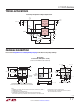
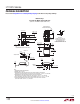
Adjustable Operation
The LT1965 adjustable version has an output voltage range
of 1.20V to 19.5V. Figure 2 illustrates that the ratio of
two external resistors sets the output voltage. The device
servos the output to maintain the ADJ pin voltage at 1.20V
referenced to ground. R1’s current equals 1.20V/R1. R2’s
current equals R1’s current plus the ADJ pin bias current.
The ADJ pin bias current, 1.3µA at 25°C, flows through
R2 into the
ADJ pin. Use the formula in Figure 2 to calcu-
late output voltage. Linear Technology recommends that
R1’s value be less than 12.1k to minimize output voltage
errors due to the ADJ pin bias current. In shutdown, the
output turns off and the divider current is zero. For curves
depicting ADJ Pin Voltage vs Temperature and ADJ Pin
Bias Current vs Temperature, see the Typical Performance
Characteristics section.
The adjustable device is tested and specified with the ADJ
pin tied to the OUT pin for an output voltage of 1.20V.
Specifications for output voltages greater than 1.20V are
proportional to the ratio of the desired output voltage to
1.20V: V
OUT
/1.20V. For example, load regulation for an
output current change of 1mA to 1.1A is typically –4.25mV
at V
OUT
= 1.20V. At V
OUT
= 5V, load regulation is:
5V
1.20V
• – 4.25mV = – 17.71mV
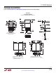
Output Capacitance
The LT1965’s design is stable with a wide range of out
-
put capacitors. The ESR of the output capacitor affects
stability, most notably with small capacitors. A minimum
output capacitor of 10µF with an ESR of 0.3W or less is
recommended to prevent oscillations. The LT1965 is a low
quiescent current device and output load transient response
is a function of output capacitance. Larger values of output
capacitance decrease the peak deviations and provide
improved transient response for larger current changes.
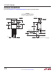
Ceramic capacitors require extra consideration. Manufac
-
turers make ceramic capacitors with a variety of dielectrics,
each with different behavior across temperature and applied
voltage. The most common dielectrics used are specified
with EIA temperature characteristic codes of Z5U, Y5V,
X5R and X7R. The Z5U and Y5V dielectrics provide high
C-V products in a small package at low cost, but exhibit
strong voltage and temperature coefficients as shown in
Figures 3 and 4. When used with a 5V regulator, a 16V
10µF Y5V capacitor can exhibit an effective value as low
as 1µF to 2µF for the DC bias applied and over
the operat-
ing temperature range. The X5R and X7R dielectrics yield
much more stable characteristics and are more suitable
for use as the output capacitor. The X7R type works over
a wider temperature range and has better temperature
stability whereas X5R is less expensive and is available in
higher values. Care still must be exercised when using X5R
and X7R capacitors; the X5R and X7R codes only specify
operating temperature range and maximum capacitance
change over temperature. Capacitance change due to DC
bias with X5R and X7R capacitors is better than Y5V and
Z5U capacitors, but can still be significant enough to drop
capacitor values below appropriate levels. Capacitor DC
bias characteristics tend to improve as component case
size increases, but expected capacitance at operating
voltages should be verified.
Figure 2. Adjustable Operation
IN
1965 F02
R2
OUT
V
IN
V
OUT
ADJ
GND
LT1965
R1
+
V
OUT
= 1.20V 1+
R2
R1
+ I
ADJ
•R2
V
ADJ
= 1.20V
I
ADJ
= 1.3µA AT 25ºC
OUTPUT RANGE = 1.20V TO19.5V