
Datasheet

LT1999-10/LT1999-20/
LT1999-50
15
1999fb
applicaTions inForMaTion
Input Common Mode Range
The LT1999 was optimized for high common mode re-
jection. Its input stage is balanced and fully differential,
designed to amplify differential signals and reject common
mode signals. There is negligible crossover distortion due
to sense voltage reversals. The amplifier is most linear in
the zero-sense region.
With the V
+
supply configured within the specified and
tested range (4.5V < V
+
< 5.5V), the LT1999’s common
mode range extends from –5V to 80V. Pushing +IN and
–IN beyond the limits specified in the Absolute Maximum
table can turn on the voltage clamps designed to protect
the +IN and –IN pins during ESD events.
It is possible to operate the LT1999 on power supplies
as low as 4V (although it is not tested or specified below
4.5V). Operating the LT1999 on supplies below 4V will
produce erratic behavior. When operating the LT1999
with supplies as low as 4V, the common mode range for
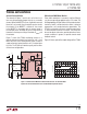
inputs which extend below GND is reduced. Refer to the
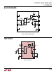
Block Diagram (Figure 1). For inputs driven below V
+
,
diode D1 conducts. For proper operation, the input to the
transconductor V(G
+
IN
) must be biased at approximately
2.25V above the GND pin. V(G
+
IN
) sits on the centertap
of a voltage divider comprised of R
+
S
and R
+
IN
V(G
–
IN
)
likewise sits in the middle of the voltage divider comprised
of R
–
S
, and R
–
IN
). The voltage on V(G
+
IN
) input is given
by the following equation:
V(G
+IN
) = V
+IN
•
R
+S
R
+S
+ R
+IN
+ V
+
−V
D1
(
)
•
R
+IN
R
+S
+ R
+IN
Setting V(G
+
IN
) = 2.25V, the ratio (R
+
IN
/R
+
S
) to 5, and V
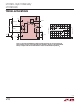
D1
equal to 0.8V (cold temperatures), a plot of the lower input
common mode range plotted against supply is shown in
Figure 3.
Output Common Mode Range
The LT1999’s output common mode level is set by the
voltage on the REF pin. The REF pin sits in the middle of
a 160k to 160k voltage divider connected between V
+
and
GND which sets the default open circuit potential of the
REF pin to mid-supply. It can be overdriven by an external
voltage source capable of driving 80k tied to a mid-supply
potential. See the Electrical Characteristics table for the
REF pin’s specified input voltage range.
Differential sampling of the OUT pin with respect the REF
pin provides the best noise immunity. Measurements of
the output voltage made differentially with respect to the
REF pin will provide the highest power supply and com-
mon mode rejection. Otherwise, power supply or GND pin
disturbances are divided by the REF pin’s voltage divider
and appear directly at the noninverting input of the trans-
resistance amplifier A
O
and are not rejected.
If not driven by a low impedance (<100Ω), the REF pin
should be filtered with at least 1nF of capacitance to a
low impedance, low noise ground plane. This external
capacitance will also provide a charge reservoir during
high frequency sampling of the REF pin by ADC inputs
attached to this pin.
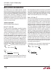
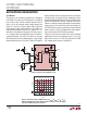
Figure 3. Lower Input Common Mode vs Supply Voltage
SUPPLY VOLTAGE (V)
4
V
CM(LOWER LIMIT)
(V)
–2.0
–2.5
–3.0
–4.0
–5.0
–3.5
–4.5
–5.5
–6.0
4.754.25 5.25
1999 F03
5.54.5 5
BELOW GROUND INPUT
COMMON MODE RANGE
LIMITED BY V
+
SUPPLY VOLTAGE
BELOW GROUND INPUT
COMMON MODE RANGE
LIMITED BY ESD CLAMPS
TYPICAL ESD CLAMP VOLTAGE