
Datasheet


LT3014
9
3014fd
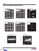
Figure 2. Ceramic Capacitor DC Bias Characteristics
Table 1. SOT-23 Measured Thermal Resistance
COPPER AREA
BOARD AREA
THERMAL RESISTANCE
(JUNCTION-TO-AMBIENT)TOPSIDE BACKSIDE
2500 sq mm 2500 sq mm 2500 sq mm 125°C/W
1000 sq mm 2500 sq mm 2500 sq mm 125°C/W
225 sq mm 2500 sq mm 2500 sq mm 130°C/W
100 sq mm 2500 sq mm 2500 sq mm 135°C/W
50 sq mm 2500 sq mm 2500 sq mm 150°C/W
Voltage and temperature coeffi cients are not the only
sources of problems. Some ceramic capacitors have a
piezoelectric response. A piezoelectric device generates
voltage across its terminals due to mechanical stress, simi-
lar to the way a piezoelectric accelerometer or microphone
works. For a ceramic capacitor the stress can be induced
by vibrations in the system or thermal transients.
For surface mount devices, heat sinking is accomplished
by using the heat spreading capabilities of the PC board
and its copper traces. Copper board stiffeners and plated
through-holes can also be used to spread the heat gener-
ated by power devices.
The following table lists thermal resistance for several
different board sizes and copper areas. All measurements
were taken in still air on 3/32” FR-4 board with one ounce
copper.
APPLICATIONS INFORMATION
Figure 3. Ceramic Capacitor Temperature Characteristics
Table 2. DFN Measured Thermal Resistance
COPPER AREA
BOARD AREA
THERMAL RESISTANCE
(JUNCTION-TO-AMBIENT)TOPSIDE BACKSIDE
2500 sq mm 2500 sq mm 2500 sq mm 40°C/W
1000 sq mm 2500 sq mm 2500 sq mm 45°C/W
225 sq mm 2500 sq mm 2500 sq mm 50°C/W
100 sq mm 2500 sq mm 2500 sq mm 62°C/W
For the DFN package, the thermal resistance junction-to-
case (θ
JC
), measured at the Exposed Pad on the back of
the die, is 16°C/W.
DC BIAS VOLTAGE (V)
CHANGE IN VALUE (%)
3014 F02
20
0
–20
–40
–60
–80
–100
0
4
8
10
26
12
14
X5R
Y5V
16
BOTH CAPACITORS ARE 16V,
1210 CASE SIZE, 10μF
TEMPERATURE (oC)
–50
40
20
0
–20
–40
–60
–80
–100
25 75
3014 F03
–25 0
50 100 125
Y5V
CHANGE IN VALUE (%)
X5R
BOTH CAPACITORS ARE 16V,
1210 CASE SIZE, 10μF
Thermal Considerations
The power handling capability of the device will be limited
by the maximum rated junction temperature (125°C). The
power dissipated by the device will be made up of two
components:
1. Output current multiplied by the input/output voltage
differential: I
OUT
• (V
IN
– V
OUT
) and,
2. GND pin current multiplied by the input voltage:
I
GND
• V
IN
.
The GND pin current can be found by examining the GND
Pin Current curves in the Typical Performance Character-
istics. Power dissipation will be equal to the sum of the
two components listed above.
The LT3014 regulator has internal thermal limiting de-
signed to protect the device during overload conditions.
For continuous normal conditions the maximum junction
temperature rating of 125°C must not be exceeded. It is
important to give careful consideration to all sources of
thermal resistance from junction to ambient. Additional
heat sources mounted nearby must also be considered.
Downloaded from Arrow.com.Downloaded from Arrow.com.Downloaded from Arrow.com.Downloaded from Arrow.com.Downloaded from Arrow.com.Downloaded from Arrow.com.Downloaded from Arrow.com.Downloaded from Arrow.com.Downloaded from Arrow.com.