
Datasheet


LT3015 Series
14
3015fb
PIN FUNCTIONS
IN (Pins 1, 2, Exposed Pad Pin 9 / 1, 2, 3, 4, Exposed
Pad Pin 13 / 3, Tab / 3, Tab ): Input. These pins supply
power to the regulator. The Tab of the DD-Pak, TO-220 and
the exposed backside pad of the DFN and MSOP packages
is an electrical connection to IN and to the device’s sub-
strate. For proper electrical and thermal performance, tie
all IN pins together and tie IN to the exposed backside or
Tab of the relevant package on the PCB. See the Applica-
tions Information Section for thermal considerations and
calculating junction temperature. The LT3015 requires
a bypass capacitor at IN. In general, a battery’s output
impedance rises with frequency, so include a bypass ca-
pacitor in battery powered applications. An input bypass
capacitor in the range of 1µF to 10µF generally suffices,
but applications with large load transients may require
higher input capacitance to prevent input supply droop
and prevent the regulator from entering dropout.
SHDN (Pin 3 / 5 / 1 / 1): Shutdown. Use the SHDN pin to
put the LT3015 into a micropower shutdown state. The
SHDN function is bi-directional, allowing use of either
positive or negative logic. The SHDN pin threshold volt-
ages are referenced to GND. The output of the LT3015 is
OFF if the SHDN pin is pulled typically within ±0.73V of
GND. Driving the SHDN pin typically more than ±1.21V
turns the LT3015 ON. Drive the SHDN pin with either a
logic gate or with open collector/drain logic using a pull-up
resistor. The resistor supplies the pull-up current of the
open collector/drain gate, typically several microamperes.
The typical SHDN pin current is 2.8µA out of the pin (for
negative logic) or 17µA into the pin (for positive logic). If
the SHDN function is unused, connect the SHDN pin to
V
IN
to turn the device ON. If the SHDN pin is floated, then
the LT3015 is OFF. A parasitic diode exists between SHDN
and IN of the LT3015. Therefore, do not drive the SHDN
pin more than 0.3V below IN during normal operation or
during a fault condition. The SHDN pin can also be used
to set a programmable undervoltage lockout (UVLO)
threshold for the regulator input supply.
GND (Pins 4, 5 / 6, 7 / 2 / 2): Ground. Tie all GND pin(s)
together and tie the bottom of the output voltage setting
resistor divider directly to the GND pin(s) for optimum
load regulation performance.
ADJ (Pin 6 / 8 / 4 / 4): Adjust. For the adjustable voltage
version, this pin is the error amplifier’s non-inverting input.
It has a typical bias current of 30nA that flows into the
pin. The ADJ pin reference voltage is –1.22V referred to
GND, and the output voltage range is –1.22V to –29.5V. A
parasitic substrate diode exists between ADJ and IN of the
LT3015. Therefore, do not drive ADJ more than 0.3V below
IN during normal operation or during a fault condition.
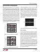
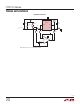
SENSE (Pin 6 / 8 / 4 / 4): Sense. For the fixed voltage ver-
sions of the LT3015 (LT3015-2.5/LT3015-3/LT3015-3.3/
LT3015-5/LT3015-12/LT3015-15), the SENSE pin connects
to the non-inverting input of the error amplifier through
an internal resistor divider network. Optimum regulation
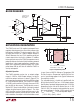
is obtained when the SENSE pin is connected to the OUT
pin of the regulator. In critical applications, small voltage
drops are caused by the resistance (R
P
) of PCB traces
between the regulator and the load. These drops can be
eliminated by connecting the SENSE pin to the output at
the load as shown in Figure 1 (Kelvin Sense Connection).
Note that the voltage drop across the external PCB traces
will add to the dropout voltage of the regulator. The SENSE
pin bias current is 100µA at the nominal output voltage. A
parasitic diode exists between SENSE and IN of the LT3015.
Therefore, do not drive SENSE more than 0.3V below IN
during normal operation or during a fault condition.
OUT (Pins 7, 8 / 9, 10, 11, 12 / 5 / 5): Output. These
pins supply power to the load. Tie all OUT pins together
for best performance. Use a minimum output capacitor
of 10µF with an ESR less than 500mΩ to prevent oscil-
lations. Large load transient applications require larger
output capacitors to limit peak voltage transients. See
the Applications Information section for more information
on output capacitance. A parasitic substrate diode exists
between OUT and IN of the LT3015. Therefore, do not drive
OUT more than 0.3V below IN during normal operation or
during a fault condition.
(DFN/MSOP/Q/T)
Figure 1. Kelvin Sense Connection
GND
LT3015-XX
SENSE
OUT
SHDN
IN
V
IN
R
P
R
P
3015 F01
LOAD