
Datasheet


LT3015 Series
15
3015fb
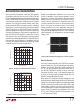
BLOCK DIAGRAM
–1.20V
1.21V
V
REF
+
–
ADJ
I LIMIT FOLDBACK
NPN DRIVER
BIAS CIRCUITRY
ADJ PIN BIAS CURRENT
COMPENSATION
QPOWER
3015 BD
V
TH
R
SNS
+
_
+
–
–
+
ERROR AMP
–
+
I LIMIT AMP
IN
OUT
SHDN
GND
R2*
R1*
*SEE TABLE 1 FOR
NOMINAL VALUES
OF R1 AND R2
SENSE
The LT3015 series are 1.5A negative low dropout linear
regulators featuring precision current limit and precision
bi-directional shutdown. The device supplies up to 1.5A
of output load current at a typical dropout voltage of
310mV. Moreover, the low 1.1mA operating quiescent
current drops to less than 1µA in shutdown. In addition
to low quiescent current, the LT3015 incorporates several
protection features that make it ideal for battery powered
applications. In dual supply applications where the regu-
lator’s load is returned to a positive supply, OUT can be
pulled above GND by 30V and still allow the LT3015 to
start up and operate.
Adjustable Operation
The LT3015 adjustable version has an output voltage
range of –1.22V to –29.3V. Output voltage is set by the
ratio of two external resistors as shown in Figure 2. The
device regulates the output to maintain the ADJ pin voltage
to –1.22V referred to ground. The current in R1 equals
–1.22V/R1 and the current in R2 equals the current in R1
plus the ADJ pin bias current. The ADJ pin bias current,
30nA at 25°C, flows into the ADJ pin. Calculate the output
voltage using the formula shown in Figure 1. The value
of R1 should be less than 50k to minimize errors in the
output voltage created by the ADJ pin bias current. Note
that in shutdown, the output is off and the divider current
APPLICATIONS INFORMATION
is zero. Curves of ADJ Pin Voltage vs Temperature, ADJ
Pin Bias Current vs Temperature and ADJ Pin Bias Cur-
rent vs Input Voltage appear in the Typical Performance
Characteristics section.
The adjustable device is tested and specified with the
ADJ pin tied to the OUT pin for a –1.22V output voltage.
Specifications for output voltages greater than –1.22V are
proportional to the ratio of the desired V
OUT
to –1.22V
(V
OUT
/–1.22V). For example, load regulation for an out-
put current change of –1mA to –1.5A is typically 2mV at
V
OUT
= –1.22V. At V
OUT
= –5V, load regulation equals:
(–5V/–1.22V)•(2mV)=8.2mV
GND
LT3015
ADJ
OUT
SHDN
IN
V
OUT
C
IN
V
IN
R1
R2
C
OUT
3015 F02
Figure 2. Adjustable Operation
V
OUT
= –1.22V 1+
R2
R1
+ I
ADJ
( )
R2
( )
V
ADJ
= –1.22V ANDI
ADJ
= 30nA AT 25°C
OUTPUT RANGE= –1.22 TO –29.5V