
Datasheet


LT3045
5
Rev. B
For more information www.analog.com
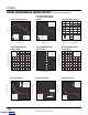
TYPICAL PERFORMANCE CHARACTERISTICS
Offset Voltage SET Pin Current Offset Voltage (V
OUT
– V
SET
)
SET Pin Current SET Pin Current Offset Voltage (V
OUT
– V
SET
)
T
J
= 25°C, unless otherwise noted.
ELECTRICAL CHARACTERISTICS
Note 9: The LT3045 is tested and specified under pulsed load conditions
such that T
J
≈ T
A
. The LT3045E is 100% tested at 25°C and performance
is guaranteed from 0°C to 125°C. Specifications over the –40°C to 125°C
operating temperature range are assured by design, characterization, and
correlation with statistical process controls. The LT3045I is guaranteed
over the full –40°C to 125°C operating temperature range. LT3045H is
100% tested at the 150°C operating junction temperature. LT3045MP
is 100% tested and guaranteed over the full −55°C to 150°C operating
temperature range. High junction temperatures degrade operating lifetimes.
Operating lifetime is derated at junction temperatures greater than 125°C.
Note 10: Parasitic diodes exist internally between the ILIM, PG, PGFB, SET,
OUTS, and OUT pins and the GND pin. Do not drive these pins more than
0.3V below the GND pin during a fault condition. These pins must remain at
a voltage more positive than GND during normal operation.
Note 11: The current limit programming scale factor is specified while the
internal backup current limit is not active. Note that the internal current
limit has foldback protection for V
IN
– V
OUT
differentials greater than 12V.
Note 12: The internal back-up current limit circuitry incorporates foldback
protection that decreases current limit for V
IN
– V
OUT
> 12V. Some level of
output current is provided at all V
IN
– V
OUT
differential voltages. Consult the
Typical Performance Characteristics graph for current limit vs V
IN
– V
OUT
.
Note 13: For output voltages less than 1V, the LT3045 requires a 10µA
minimum load current for stability.
Note 14: Maximum OUT-to-OUTS differential is guaranteed by design.
Note 15: MP-Grade is only offered in the DFN package.
V
IN
= 2V
I
L
= 1mA
V
OUT
= 1.3V
TEMPERATURE (°C)
–75
–50
–25
0
25
50
75
100
125
150
99.0
99.2
99.4
99.6
99.8
100.0
100.2
100.4
100.6
100.8
101.0
SET PIN CURRENT (µA)
3045 G01
N = 3250
I
SET
DISTRIBUTION (µA)
98
99
100
101
102
3045 G02
V
IN
= 2V
I
L
= 1mA
V
OUT
= 1.3V
TEMPERATURE (°C)
–75
–50
–25
0
25
50
75
100
125
150
–2.0
–1.5
–1.0
–0.5
0
0.5
1.0
1.5
2.0
OFFSET VOLTAGE (mV)
3045 G03
N = 3250
V
OS
DISTRIBUTION (mV)
–2
–1
0
1
2
3045 G04
I
L
= 1mA
V
OUT
= 1.3V
150°C
125°C
25°C
–55°C
INPUT VOLTAGE (V)
0
2
4
6
8
10
12
14
16
18
20
99.0
99.2
99.4
99.6
99.8
100.0
100.2
100.4
100.6
100.8
101.0
SET PIN CURRENT (µA)
3045 G05
I
L
= 1mA
V
OUT
= 1.3V
150°C
125°C
25°C
–55°C
INPUT VOLTAGE (V)
0
2
4
6
8
10
12
14
16
18
20
–2.0
–1.5
–1.0
–0.5
0
0.5
1.0
1.5
2.0
OFFSET VOLTAGE (mV)
3045 G06
Downloaded from Arrow.com.Downloaded from Arrow.com.Downloaded from Arrow.com.Downloaded from Arrow.com.Downloaded from Arrow.com.