
Datasheet

LT3050 Series
20
3050fa
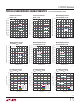
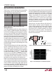
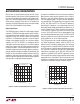
Figure 6. Noise Resulting from Tapping on a Ceramic Capacitor
10ms/DIV
V
OUT
1mV/DIV
3050 F06
V
OUT
= 5V
C
OUT
= 10µF
C
REF/BYP
= 10nF
APPLICATIONS INFORMATION
Voltage and temperature coeffi cients are not the only
sources of problems. Some ceramic capacitors have a
piezoelectric response. A piezoelectric device generates
voltage across its terminals due to mechanical stress,
similar to the way a piezoelectric accelerometer or micro-
phone works. For a ceramic capacitor, the stress is induced
by vibrations in the system or thermal transients. The
resulting voltages produced cause appreciable amounts
of noise. A ceramic capacitor produced the trace in
Figure 6 in response to light tapping from a pencil. Similar
vibration induced behavior can masquerade as increased
output voltage noise.
Overload Recovery
Like many IC power regulators, the LT3050 has safe oper-
ating area protection. The safe area protection decreases
current limit as input-to-output voltage increases, and
keeps the power transistor inside a safe operating region
for all values of input-to-output voltage. The LT3050 pro-
vides some output current at all values of input-to-output
voltage up to the device breakdown.
When power is fi rst applied, the input voltage rises and the
output follows the input; allowing the regulator to start-up
into very heavy loads. During start-up, as the input voltage
is rising, the input-to-output voltage differential is small,
allowing the regulator to supply large output currents.
With a high input voltage, a problem can occur wherein
the removal of an output short will not allow the output
to recover. Other regulators, such as the LT1083/LT1084/
LT1085 family and LT1764A also exhibit this phenomenon,
so it is not unique to the LT3050. The problem occurs with
a heavy output load when the input voltage is high and the
output voltage is low. Common situations are: immediately
after the removal of a short-circuit or if the shutdown pin
is pulled high after the input voltage is already turned on.
The load line for such a load intersects the output cur-
rent curve at two points. If this happens, there are two
stable output operating points for the regulator. With this
double intersection, the input power supply needs to be
cycled down to zero and brought up again to make the
output recover.
Thermal Considerations
The LT3050’s maximum rated junction temperature of
125°C limits its power handling capability. Two components
comprise the power dissipated by the device:
1. Output current multiplied by the input/output
voltage differential: I
OUT
• (V
IN
– V
OUT
), and
2. GND pin current multiplied by the input voltage:
I
GND
• V
IN
GND pin current is determined using the GND Pin Current
curves in the Typical Performance Characteristics section.
Power dissipation equals the sum of the two components
listed above.
The LT3050 regulator has internal thermal limiting that
protects the device during overload conditions. For con-
tinuous normal conditions, do not exceed the maximum
junction temperature of 125°C. Carefully consider all
sources of thermal resistance from junction-to-ambient
including other heat sources mounted in proximity to the
LT3050.
The undersides of the LT3050 DFN and MSOP packages
have exposed metal from the lead frame to the die attach-
ment. These packages allow heat to directly transfer from
the die junction to the printed circuit board metal to control
maximum operating junction temperature. The dual-in-line
pin arrangement allows metal to extend beyond the ends
of the package on the topside (component side) of a PCB.
Connect this metal to GND on the PCB. The multiple IN
and OUT pins of the LT3050 also assist in spreading heat
to the PCB.