
Datasheet


LT3060 Series
21
3060fb
applicaTions inForMaTion
The LT3060 IN pin withstands reverse voltages up to 50V.
The device limits current flow to less than 300µA (typi-
cally less than 50µA) and no negative voltage appears at
OUT. The device protects both itself and the load against
batteries that are plugged in backwards.
The SHDN pin cannot be driven below GND unless tied to
the IN pin. If the SHDN pin is driven below GND while IN is
powered, the output may turn on. SHDN pin logic cannot
be referenced to a negative supply voltage.
The LT3060 incurs no damage if its output is pulled be-
low ground. If the input is left open-circuit or grounded,
the output can be pulled below ground by 50V. No cur-
rent flows through the pass transistor from the output.
However, current flows in (but is limited by) the resistor
divider that sets the output voltage. Current flows from
the bottom resistor in the divider and from the ADJ pin’s
internal clamp through the top resistor in the divider to
the external circuitry pulling OUT below ground. If the
input is powered by a voltage source, the output sources
current equal to its current limit capability and the LT3060
protects itself by thermal limiting. In this case, grounding
the SHDN pin turns off the device and stops the output
from sourcing current.
The LT3060 incurs no damage if the ADJ pin is pulled
above or below ground by less than 50V. For the adjust-
able version, if the input is left open-circuit or grounded,
the ADJ pin performs like a large resistor (typically 30k)
in series with a diode when pulled below ground, and like
30k in series with two diodes when pulled above ground.
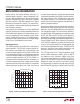
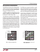
In circuits where a backup battery is required, several
different input/output conditions can occur. The output
voltage may be held up while the input is either pulled to
ground, pulled to some intermediate voltage or left open-
circuit. Current flow back into the output follows the curve
shown in Figures 7 and 8.
If the LT3060’s IN pin is forced below the OUT pin or the
OUT pin is pulled above the IN pin, input current typically
drops to less than 1µA. This occurs if the LT3060 input
is connected to a discharged (low voltage) battery and
either a backup battery or a second regulator holds up
the output. The state of the SHDN pin has no effect on
the reverse current if the output is pulled above the input.
OUTPUT VOLTAGE (V)
0
0
REVERSE OUTPUT CURRENT (mA)
1.4
1.6
1.8
1.2
1.0
0.8
0.4
0.6
0.2
2.0
5 30 35 40 4510 15 20
3060 F07
25
ADJ
OUT
T
J
= 25°C
V
IN
= 0V
CURRENT FLOWS
INTO OUT PIN
V
OUT
= V
ADJ
Figure 7. LT3060 Reverse Output Current Figure 8. LT3060-1.2/-1.5/-1.8/-2.5/-3.3/-5
Reverse Output Current
OUTPUT VOLTAGE (V)
0
0
REVERSE OUTPUT CURRENT (µA)
250
150
200
100
50
350
300
5 30 35 40 4510 15 20
3060 F08w
25
LT3060-1.2
LT3060-5
LT3060-1.5
LT3060-1.8
LT3060-2.5
LT3060-3.3
T
J
= 25°C
V
IN
= 0V
V
OUT
= 1.5V
V
OUT
= 1.2V
V
OUT
= 0.6V
V
OUT
= 1.8V
V
OUT
= 2.5V
V
OUT
= 3.3V
V
OUT
= 5V