
Datasheet

LT3060 Series
19
3060fb
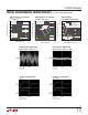
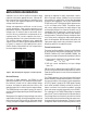
4ms/DIV
3060 F06
V
OUT
500µV/DIV
V
OUT
= 0.6V
C
OUT
= 10µF
C
REF/BYP
= 10nF
I
LOAD
= 100mA
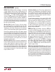
Figure 6. Noise Resulting from Tapping on a Ceramic Capacitor
applicaTions inForMaTion
capacitors, but can still be significant enough to drop
capacitor values below appropriate levels. Capacitor DC
bias characteristics tend to improve as component case
size increases, but expected capacitance at operating
voltage should be verified.
Voltage and temperature coefficients are not the only
sources of problems. Some ceramic capacitors have a
piezoelectric response. A piezoelectric device generates
voltage across its terminals due to mechanical stress,
similar to the way a piezoelectric accelerometer or mi-
crophone works. For a ceramic capacitor, the stress is
induced by vibrations in the system or thermal transients.
The resulting voltages produced cause appreciable
amounts of noise. A ceramic capacitor produced the trace
in Figure 6 in response to light tapping from a pencil.
Similar vibration induced behavior can masquerade as
increased output voltage noise.
allowing the regulator to supply large output currents.
With a high input voltage, a problem can occur wherein
the removal of an output short will not allow the output
to recover. Other regulators, such as the LT1083/LT1084/
LT1085 family and LT1764A also exhibit this phenomenon,
so it is not unique to the LT3060. The problem occurs
with a heavy output load when the input voltage is high
and the output voltage is low. Common situations are: (1)
immediately after the removal of a short-circuit or (2) if
the shutdown pin is pulled high after the input voltage is
already turned on. The load line intersects the output current
curve at two points creating two stable output operating
points for the regulator. With this double intersection, the
input power supply needs to be cycled down to zero and
brought up again for the output to recover.
Thermal Considerations
The power handling capability of the device will be limited
by the maximum rated junction temperature (125°C for
LT3060E, LT3060I or 150°C for LT3060MP, LT3060H). Two
components comprise the power dissipated by the device:
1. Output current multiplied by the input/output voltage
differential: I
OUT
• (V
IN
–V
OUT
), and
2. GND pin current multiplied by the input voltage:
I
GND
• V
IN
GND pin current is determined using the GND Pin Current
curves in the Typical Performance Characteristics section.
Power dissipation equals the sum of the two components
listed above.
The LT3060 regulators have internal thermal limiting that
protects the device during overload conditions. For continu-
ous normal conditions, the maximum junction temperature
of 125°C (E-grade, I-grade) or 150°C (MP-grade, H-grade)
must not be exceeded. Carefully consider all sources of
thermal resistance from junction-to-ambient including
other heat sources mounted in proximity to the LT3060.
The underside of the LT3060 DFN package has exposed
metal (1mm
2
) from the lead frame to the die attachment.
The package allows heat to directly transfer from the die
junction to the printed circuit board metal to control maxi-
mum operating junction temperature. The dual-in-line pin
arrangement allows metal to extend beyond the ends of
Overload Recovery
Like many IC power regulators, the LT3060 has safe
operating area protection. The safe operating area protec-
tion decreases current limit as input-to-output voltage
increases, and keeps the power transistor inside a safe
operating region for all values of input-to-output voltage.
The LT3060 provides some output current at all values of
input-to-output voltage up to the specified 45V operational
maximum.
When power is first applied, the input voltage rises and the
output follows the input; allowing the regulator to start-up
into very heavy loads. During start-up, as the input voltage
is rising, the input-to-output voltage differential is small,