
Datasheet


LT3090
19
3090fa
For more information www.linear.com/LT3090
applicaTions inForMaTion
In summary, the GND pin of LT3090 is highly versatile
and can be tied to different places depending on the ap-
plication’s requirements:
a) It can be tied to the system
GND for low dropout operation for output voltages greater
than –1.6V, b) it can be tied to a positive voltage for low
dropout operation for very low output voltages, and c) as
illustrated in the Floating 3-Terminal Regulator section, the
GND pin can be tied to the OUT pin for very high common
mode voltage applications.
Direct Paralleling
Higher output current is obtained by paralleling multiple
LT3090s. Tie all SET pins together and all IN pins together.
Connect the OUT pins together using small pieces of PC
trace (used as a ballast resistor) to equalize the currents
in each LT3090. PC trace resistance in mΩ/inch is shown
in Table 2. Ballasting requires only a tiny area.
Table 2. PC Board Trace Resistance
WEIGHT (oz) 10mil WIDTH* 20mil WIDTH*
1 54.3 27.1
2 27.1 13.6
*Trace resistance is measured in mΩ/in
The small worst-case offset of ±2mV for each paralleled
LT3090 minimizes the value of required ballast resistance.
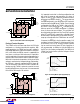
Figure 16 illustrates that two LT3090s, each using a 20mΩ
PCB trace ballast resistor, provide better than 80% output
current sharing at full load. The 20mΩ external resistances
(10mΩ for the two devices in parallel) only adds 12mV of
output regulation drop with a 1.2A maximum load. With
an output voltage as low as –1.2V, this only adds 1% to
the regulation accuracy. If this additional load regulation
error is intolerable, circuits shown in the Typical Applica
-
tions section
highlight how to correct this error using
the output current monitor function or the master-slave
configuration.
Finally, note that more than two LT3090s can be paralleled
for higher output current. Paralleling multiple LT3090s is
a useful technique for distributing heat on the PCB. For
applications with high input-to-output voltage differential,
either input series resistors or resistors in parallel with
the LT3090s further spread heat.
Thermal Considerations
The LT3090 has internal power and thermal limiting cir
-
cuitry designed to
protect
it under overload conditions. The
typical thermal shutdown temperature is 165°C with about
8°C of hysteresis. For continuous normal load conditions,
do not exceed the maximum junction temperature. It is
important to consider all sources of thermal resistance
from junction to ambient. This includes junction-to-case,
case-to-heat sink interface, heat sink resistance or circuit
board-to-ambient as the application dictates. Additionally,
consider all heat sources in close proximity to the LT3090.
The undersides of the DFN and MSOP packages have
exposed metal from the lead frame to the die attachment.
Both packages allow heat to directly transfer from the die
junction to the PCB metal to limit the maximum operating
Figure 16. Parallel Devices
LT3090
V
OUT
–2.5V
MAX I
OUT
1.2A
GND
ILIM
SHDN
–
+
50µA
SET
OUT
IMONN
10µF
24.9k
IN
V
IN
–3V TO –10V
IMONP
10k
10µF
20m
0.1µF
3090 F16
LT3090
GND
ILIM
SHDN
–
+
50µA
SET
OUT
IMONN
IN
IMONP
10k
20m
Downloaded from Arrow.com.Downloaded from Arrow.com.Downloaded from Arrow.com.Downloaded from Arrow.com.Downloaded from Arrow.com.Downloaded from Arrow.com.Downloaded from Arrow.com.Downloaded from Arrow.com.Downloaded from Arrow.com.Downloaded from Arrow.com.Downloaded from Arrow.com.Downloaded from Arrow.com.Downloaded from Arrow.com.Downloaded from Arrow.com.Downloaded from Arrow.com.Downloaded from Arrow.com.Downloaded from Arrow.com.Downloaded from Arrow.com.Downloaded from Arrow.com.