
Datasheet


LT3092
8
3092fb
Introduction
The LT3092 is a versatile IC that operates as a 2-terminal
programmable current source with the addition of only
two external resistors; no external bypass capacitors are
needed for stability.
The LT3092 is easy to use and has all the protection fea-
tures expected in high performance products. Included
are reverse-voltage protection, reverse-current protec-
tion, short-circuit protection and thermal shutdown with
hysteresis.
The LT3092 operates with or without input and output
capacitors. The simplest current source application
requires only two discrete resistors to set a constant
output current up to 200mA. A variety of analog tech-
niques lend themselves to regulating and varying the
current source value.
The device utilizes a precision “0” TC 10A reference cur-
rent source to program output current. This 10µA current
source connects to the noninverting input of a power
operational amplifi er. The power operational amplifi er
provides a low impedance buffered output of the voltage
on the noninverting input.
Many application areas exist in which operation without
input and output capacitors is advantageous. A few of
these applications include sensitive circuits that cannot
endure surge currents under fault or overload conditions
and intrinsic safety applications in which safety regulations
limit energy storage devices that may spark or arc.
Programming Output Current in 2-Terminal
Current Source Mode
Setting the LT3092 to operate as a 2-terminal current
source is a simple matter. The 10µA reference current from
the SET pin is used with one resistor to generate a small
voltage, usually in the range of 100mV to 1V (200mV is
a level that will help reject offset voltage, line regulation,
and other errors without being excessively large). This
voltage is then applied across a second resistor that
connects from OUT to the fi rst resistor. Figure 1 shows
connections and formulas to calculate a basic current
source confi guration.
APPLICATIONS INFORMATION
With a 10A current source generating the reference that
gains up to set output current, leakage paths to or from
the SET pin can create errors in the reference and output
currents. High quality insulation should be used (e.g.,
Tefl on, Kel-F). The cleaning of all insulating surfaces to
remove fl uxes and other residues may be required. Surface
coating may be necessary to provide a moisture barrier
in high humidity environments.
Minimize board leakage by encircling the SET pin and
circuitry with a guard ring operated at a potential close
to itself; tie the guard ring to the OUT pin. Guarding
both sides of the circuit board is required. Bulk leakage
reduction depends on the guard ring width. Ten nano-
amperes of leakage into or out of the SET pin and its as-
sociated circuitry creates a 0.1% reference current error.
Leakages of this magnitude, coupled with other sources
of leakage, can cause signifi cant offset voltage and refer-
ence current drift, especially over the possible operating
temperature range.
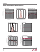
Figure 1. Using the LT3092 as a Current Source
ImA
VµAR
I
V
R
µA
OUT
SET SET
OUT
SET
OUT
≥
=
==
05
10
10
.
•
•
RR
R
SET
OUT
IN
SET OUT
+
–
LT3092
10µA
I
OUT
V
SET
R
SET
3092 F01
+
–
R
OUT
Selecting R
SET
and R
OUT
In Figure 1, both resistors R
SET
and R
OUT
program the
value of the output current. The question now arises: the
ratio of these resistors is known, but what value should
each resistor be?
The fi rst resistor to select is R
SET
. The value selected should
generate enough voltage to minimize the error caused by
the offset between the SET and OUT pins. A reasonable
starting level is 200mV of voltage across R
SET
(R
SET
equal
to 20k). Resultant errors due to offset voltage are a few
percent. The lower the voltage across R
SET
becomes, the
higher the error term due to the offset.