
Datasheet


LT137A/LM137
LT337A/LM337
4
137afb
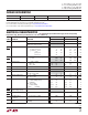
ELECTRICAL CHARACTERISTICS
The l denotes the specifi cations which apply over the full operating
temperature range, otherwise specifi cations are at T
A
= 25°C. (Notes 2, 3)
SYMBOL PARAMETER CONDITIONS
LT337A LM337
UNITSMIN TYP MAX MIN TYP MAX
V
REF
Reference Voltage
|
V
IN
– V
OUT
|
= 5V, I
OUT
= 10mA, T
j
= 25°C –1.238 –1.250 –1.262 –1.213 –1.250 –1.287 V
3V ≤
|
V
IN
– V
OUT
|
≤ 40V
10mA ≤ I
OUT
≤ I
MAX
, P ≤ P
MAX
l
–1.220 –1.250 –1.280 –1.200 –1.250 –1.300 V
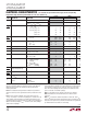
ΔV
OUT
ΔI
OUT
Load Regulation 10mA ≤ I
OUT
≤ I
MAX
, (Notes 4 and 5)
T
j
= 25°C,
|
V
OUT
|
≤ 5V
T
j
= 25°C,
|
V
OUT
|
≥ 5V
|
V
OUT
|
≤ 5V
|
V
OUT
|
≥ 5V
l
l
5
0.1
10
0.2
25
0.5
50
1
15
0.3
20
0.3
50
1
70
1.5
mV
%
mV
%
ΔV
OUT
ΔV
IN
Line Regulation 3V ≤
|
V
IN
– V
OUT
|
≤ 40V (Note 4)
T
j
= 25°C
l
0.005
0.01
0.01
0.03
0.01
0.02
0.04
0.07
%/V
%/V
Ripple Rejection V
OUT
= –10V, f = 120Hz
C
ADJ
= 0
C
ADJ
= 10μF
l
60
70
66
80 66
60
77
dB
dB
Thermal Regulation T
j
= 25°C, 10ms Pulse 0.002 0.02 0.003 0.04 %/W
I
ADJ
Adjust Pin Current
l
65 100 65 100 μA
ΔI
ADJ
Adjust Pin Current Change 10mA ≤ I
OUT
≤ I
MAX
3V ≤
|
V
IN
– V
OUT
|
≤ 40V
l
l
0.2
1
2
5
0.5
2
5
5
μA
μA
Minimum Load Current
|
V
IN
– V
OUT
|
≤ 40V
|
V
IN
– V
OUT
|
≤ 10V
l
l
2.5
1.2
5
3
2.5
1
10
6
mA
mA
I
SC
Current Limit
|
V
IN
– V
OUT
|
≤ 15V,
K, M and T Package
H Package
|
V
IN
– V
OUT
|
= 40V,
K, M and T Package
T
j
= 25°C H Package
l
l
1.5
0.5
0.24
0.15
2.2
0.8
0.5
0.25
1.5
0.5
0.15
0.1
2.2
0.8
0.4
0.17
A
A
A
A
ΔV
OUT
ΔTemp
Temperature Stability of
Output Voltage (Note 6)
l
0.6 1.5 0.6 %
ΔV
OUT
ΔTime
Long Term Stability T
A
= 125°C, 1000 Hours 0.3 1 0.3 1 %
e
n
RMS Output Noise
(% of V
OUT
)
T
A
= 25°C, 10Hz ≤ f ≤ 10kHz 0.003 0.003 %
θ
JC
Thermal Resistance Junction
to Case
H Package
K Package
M and T Package
12
2.3
3
15
3
5
12
2.3
3
15
3
5
°C/W
°C/W
°C/W
Note 1: Stresses beyond those listed under Absolute Maximum Ratings
may cause permanent damage to the device. Exposure to any Absolute
Maximum Rating condition for extended periods may affect device
reliability and lifetime.
Note 2: The shaded electrical specifi cations indicate those parameters
which have been improved or guaranteed test limits provided for the fi rst
time.
Note 3: Unless otherwise indicated, these specifi cations apply:
|
V
IN
– V
OUT
|
= 5V; and I
OUT
= 0.1A for the H package, I
OUT
= 0.5A for the K, M,
and T packages. Power dissipation is internally limited. However, these
specifi cations apply for power dissipation up to 2W for the H package and
20W for the K and T packages. I
MAX
= 1.5A for the K, M, and T packages,
and 0.2A for the H package.
Note 4: Testing is done using a pulsed low duty cycle technique. See
thermal regulation specifi cations for output changes due to heating effects.
Load regulation is measured on the output pin at a point 1/8" below the
base of the K and H package and at the junction of the wide and narrow
portion of the lead on the M and T package.
Note 5: Load regulation for the LT337AT is the same as for LM337T.
Note 6: Guaranteed on LT137A and LT337A, but not 100% tested in
production.
Note 7: I
SC
is tested at the ambient temperatures of 25°C and –55°C. I
SC
cannot be tested at the maximum ambient temperature of 150°C due to the
high power level required. I
SC
specifi cation at 150°C ambient is guaranteed
by characterization and correlation to 25°C testing.