
Datasheet


LT137A/LM137
LT337A/LM337
8
137afb
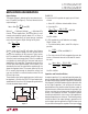
becomes shorted, due to the output capacitor discharging
into the regulator. This can be prevented by using the diode
D1 (see Figure 2) between the input and the output.
The input capacitor, C2, is only required if the regulator is
more than 4 inches from the raw supply fi lter capacitor.
Bypassing the Adjustment Pin
The adjustment pin of the LT137A may be bypassed with a
capacitor to ground, C1, to reduce output ripple, noise, and
impedance. These parameters scale directly with output
voltage if the adjustment pin is not bypassed. A bypass
capacitor reduces ripple, noise, and impedance to that of
a 1.25V regulator. In a 15V regulator, for example, these
parameters are improved by 15V/1.25V = 12 to 1. This
improvement holds only for those frequencies where the
impedance of the bypass capacitor is less than R1. Ten
microfarads is generally suffi cient for 60Hz power line
applications where the ripple frequency is 120Hz since
X
C
= 130Ω. The capacitor should have a voltage rating at
least as high as the output voltage of the regulator. Values
larger than 10μF may be used, but if the output is larger
than 25V, a diode, D2, should be added between the output
and adjustment pins (see Figure 2).
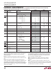
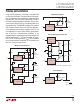
Proper Connection of Divider Resistors
The LT137A has an excellent load regulation specifi cation
of 0.5% and is measured at a point 1/8" from the bottom
of the package. To prevent degradation of load regulation,
the resistors which set output voltage, R1 and R2, must be
connected as shown in Figure 3. Note that the positive side
of the load has a true force and sense (Kelvin) connection,
but the negative side of the load does not.
R1 should be connected directly to the output lead of the
regulator, as close as possible to the specifi ed point 1/8"
from the case. R2 should be connected to the positive
side of the load separately from the positive (ground)
connection to the raw supply. With this arrangement, load
regulation is degraded only by the resistance between the
regulator output pin and the load. If R1 is connected to
the load, regulation will be degraded.
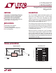
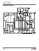
LT137A
ADJ
V
IN
–V
IN
R2
*D1 PROTECTS THE REGULATOR FROM INPUT SHORTS TO GROUND. IT IS
REQUIRED ONLY WHEN C3 IS LARGER THAN 20μF AND V
OUT
IS LARGER THAN 6V.
**D2 PROTECTS THE ADJUST PIN OF THE REGULATOR FROM OUTPUT SHORTS
IF C2 IS LARGER THAN 10μF AND V
OUT
IS LARGER THAN –25V.
D1*
1N4002
D2**
1N4002
V
OUT
–V
OUT
137A F02
+
R1
C3
+
C1
+
C2
Figure 2
LT137A
ADJ
V
IN
–V
IN
R2
CONNECT R1
DIRECTLY TO
REGULATOR PIN
LEAD RESISTANCE HERE
DEGRADES LOAD REGULATION.
MINIMIZE THE LENGTH OF
THIS LEAD.
LEAD RESISTANCE HERE DOES
NOT AFFECT LOAD REGULATION
V
OUT
137A F03
R1
LOAD
Figure 3
APPLICATIONS INFORMATION