
Datasheet


LT3435
20
3435fa
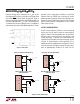
Figure 12. Suggested Layout
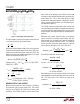
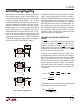
Figure 11. High Speed Switching Path
APPLICATIO S I FOR ATIO
WUUU
C2
C1
3435 F11
D1
L1
V
IN
LT3435
V
OUT
V
IN
SW
42
HIGH
FREQUENCY
CIRCULATION
PATH
+
LOAD
NC
R2
C2
C5
R1
R3
C4
SW
V
IN
V
IN
SW
BOOST
C
T
GND
16
15
14
13
12
11
10
9
1
2
3
4
5
6
7
8
PGOOD
SHDN
SYNC
PGFB
FB
V
C
BIAS
C
SS
3435 F12
C3
GND
GND
D1
L1
V
OUT
C1
C2 D2
MINIMIZE
D1-C3
LOOP
V
IN
KELVIN SENSE
FEEDBACK
TRACE AND
KEEP SEPARATE
FROM BIAS TRACE
CONNECT PIN 8 GND TO THE
PIN 17 EXPOSED PAD GND
PLACE VIA's UNDER EXPOSED
PAD TO A BOTTOM PLANE TO
ENHANCE THERMAL
CONDUCTIVITY
LT3435
parasitic inductance produces a flyback spike across the
LT3435 switch. When operating at higher currents and
input voltages, with poor layout, this spike can generate
voltages across the LT3435 that may exceed its absolute
maximum rating. A ground plane should always be used
under the switcher circuitry to prevent interplane coupling
and overall noise.
The V
C
and FB components should be kept as far away as
possible from the switch and boost nodes. The LT3435
pinout has been designed to aid in this. The ground for
these components should be separated from the switch
current path. Failure to do so will result in poor stability or
subharmonic like oscillation.
Board layout also has a significant effect on thermal
resistance. Pin 8 and the exposed die pad, Pin 17, are a
continuous copper plate that runs under the LT3435 die.
This is the best thermal path for heat out of the package.
Reducing the thermal resistance from Pin 8 and exposed
pad onto the board will reduce die temperature and in-
crease the power capability of the LT3435. This is achieved
by providing as much copper area as possible around the
exposed pad. Adding multiple solder filled feedthroughs
under and around this pad to an internal ground plane will
also help. Similar treatment to the catch diode and coil
terminations will reduce any additional heating effects.
THERMAL CALCULATIONS
Power dissipation in the LT3435 chip comes from four
sources: switch DC loss, switch AC loss, boost circuit
current, and input quiescent current. The following formu-
las show how to calculate each of these losses. These
formulas assume continuous mode operation, so they
should not be used for calculating efficiency at light load
currents.
Switch loss:
P
RI V
V
tIVf
SW
SW OUT OUT
IN
EFF OUT IN
=
()( )
+
()( )()()
2
12/
Boost current loss:
P
VI
V
BOOST
OUT OUT
IN
=
()
()
2
46/
Quiescent current loss:
P
Q
= V
IN
(0.0026) + V
OUT
(0.001)
R
SW
= switch resistance (≈0.15 when hot )
t
EFF
= effective switch current/voltage overlap time
(t
r
+ t
f
+ t
IR
+ t
IF
)
t
r
= (V
IN
/1.2)ns
t
f
= (V
IN
/1.7)ns
t
IR
= t
IF
= (I
OUT
/0.2)ns
f = switch frequency