
Datasheet


LT3470
8
3470fd
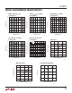
Figure 1. Operating Waveforms of the LT3470 Converting 12V to 5V Using a 33µH Inductor and 10µF Output Capacitor
The LT3470 uses a hysteretic control scheme in conjunction
with Burst Mode operation to provide low output ripple
and low quiescent current while using a tiny inductor and
capacitors.
Operation can best be understood by studying the Block
Diagram. An error amplifier measures the output voltage
through an external resistor divider tied to the FB pin. If
the FB voltage is higher than V
REF
, the error amplifier will
shut off all the high power circuitry, leaving the LT3470
in its micropower state. As the FB voltage falls, the error
amplifier will enable the power section, causing the chip
to begin switching, thus delivering charge to the output
capacitor. If the load is light the part will alternate between
micropower and switching states to keep the output in
regulation (See Figure 1a). At higher loads the part will
switch continuously while the error amp servos the top
and bottom current limits to regulate the FB pin voltage
to 1.25V (See Figure 1b).
The switching action is controlled by an RS latch and two
current comparators as follows: The switch turns on,
and the current through it ramps up until the top current
comparator trips and resets the latch causing the switch
to turn off. While the switch is off, the inductor current
ramps down through the catch diode. When both the bot-
tom current comparator trips and the minimum off-time
one-shot expires, the latch turns the switch back on thus
completing a full cycle. The hysteretic action of this control
scheme results in a switching frequency that depends
on inductor value, input and output voltage. Since the
switch only turns on when the catch diode current falls
below threshold, the part will automatically switch slower
to keep inductor current under control during start-up or
short-circuit conditions.
The switch driver operates from either the input or from
the BOOST pin. An external capacitor and internal diode
is used to generate a voltage at the BOOST pin that is
higher than the input supply. This allows the driver to
fully saturate the internal bipolar NPN power switch for
efficient operation.
If the SHDN pin is grounded, all internal circuits are turned
off and V
IN
current reduces to the device leakage current,
typically a few nA.
(1a) Burst Mode Operation (1b) Continuous Operation
V
OUT
20mV/DIV
I
L
100mA/DIV
1ms/DIV
V
OUT
20mV/DIV
I
L
100mA/DIV
5µs/DIV
3470 F01a
NO LOAD
10mA LOAD
V
OUT
20mV/DIV
I
L
100mA/DIV
1µs/DIV
V
OUT
20mV/DIV
I
L
100mA/DIV
1µs/DIV
3470 F1b
200mA LOAD
150mA LOAD
operaTion