
Datasheet


LT3471
3
3471fb
ELECTRICAL CHARACTERISTICS
Quiescent Current
vs Temperature
V
REF
Voltage vs Temperature
V
REF
Voltage vs V
REF
Current
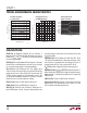
PARAMETER CONDITIONS MIN TYP MAX UNITS
SHDN Input Voltage Low Quiescent Current ≤ 1μA 0.3 V
SHDN Pin Bias Current V
SHDN
= 3V, V
IN
= 4V
V
SHDN
= 0V
22
0
36
0.1
μA
μA
The ● denotes specifi cations which apply over the full operating
temperature range, otherwise specifi cations are T
A
= 25°C. V
IN
= V
SHDN
= 3V unless otherwise noted.
Note 1: Stresses beyond those listed under Absolute Maximum Ratings
may cause permanent damage to the device. Exposure to any Absolute
Maximum Rating condition for extended periods may affect device
reliability and lifetime.
Note 2: The LT3471E is guaranteed to meet performance specifi cations
from 0°C to 70°C. Specifi cations over the –40°C to 85°C operating
temperature range are assured by design, characterization and
correlation with statistical process controls.
Note 3: Current fl ows out of the pin.
Note 4: See Typical Performance Characteristics for guaranteed current
limit vs duty cycle.
Note 5: V
CESAT
is 100% tested at wafer level only.
TYPICAL PERFORMANCE CHARACTERISTICS
TEMPERATURE (°C)
–50 –25
1.6
QUIESCENT CURRENT (mA)
2.0
2.6
0
50
75
3471 G01
1.8
2.4
2.2
25
100
125
TEMPERATURE (°C)
–50 –25
0.990
V
REF
(V)
1.000
1.010
0
50
75
3471 G02
0.995
1.005
25
100
125
V
REF
CURRENT 200μA/DIV
3471 G03
V
REF
VOLTAGE
100mV/DIV
SHDN/SS Current
vs SHDN/SS Voltage
Current Limit vs Duty Cycle
Switch Saturation Voltage
vs Switch Current
SHDN/SS VOLTAGE 1V/DIV
3471 G04
SHDN/SS
CURRENT
20μV/DIV
V
IN
= 3.3V
V
IN
> V
SHDN/SS
DUTY CYCLE (%)
0
CURRENT LIMIT (A)
1.2
1.6
2.2
2.0
80
3471 G05
0.8
0.4
1.0
1.4
1.8
0.6
0.2
0
20
40
60
100
TYPICAL
GUARANTEED
T
A
= 25°C
SW CURRENT (A)
0
V
CESAT
(mV)
800
700
600
500
400
300
200
100
0
1.6
3471 G06
0.4 0.8 1.2 2.01.40.2 0.6 1.0 1.8
90°C
25°C