
Datasheet


Table Of Contents
LT3480
8
3480fe
For more information www.linear.com/LT3480
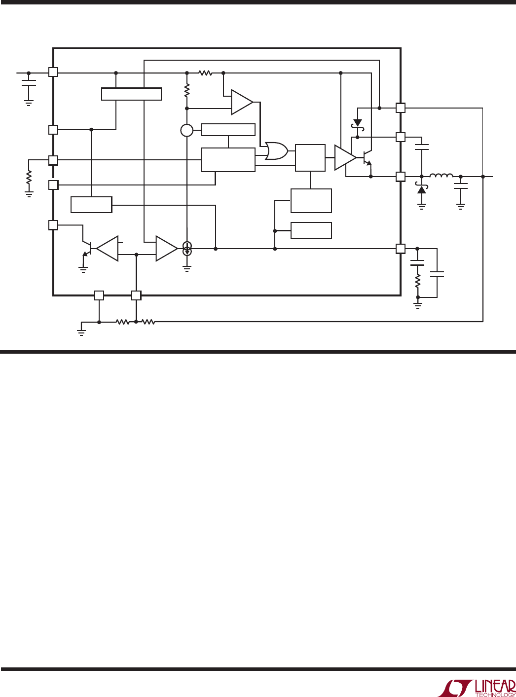
OPERATION
The LT3480 is a constant frequency, current mode step-
down regulator. An oscillator, with frequency set by RT,
enables an RS flip-flop, turning on the internal power
switch. An amplifier and comparator monitor the current
flowing between the V
IN
and SW pins, turning the switch
off when this current reaches a level determined by the
voltage at V
C
. An error amplifier measures the output
voltage through an external resistor divider tied to the FB
pin and servos the V
C
pin. If the error amplifier’s output
increases, more current is delivered to the output; if it
decreases, less current is delivered. An active clamp on the
V
C
pin provides current limit. The V
C
pin is also clamped to
the voltage on the RUN/SS pin; soft-start is implemented
by generating a voltage ramp at the RUN/SS pin using an
external resistor and capacitor.
An internal regulator provides power to the control circuitry.
The bias regulator normally draws power from the V
IN
pin,
but if the BD pin is connected to an external voltage higher
than 3V bias power will be drawn from the external source
(typically the regulated output voltage). This improves
efficiency. The RUN/SS pin is used to place the LT3480
in shutdown, disconnecting the output and reducing the
input current to less than 1µA.
The switch driver operates from either the input or from
the BOOST pin. An external capacitor and diode are used
to generate a voltage at the BOOST pin that is higher than
the input supply. This allows the driver to fully saturate the
internal bipolar NPN power switch for efficient operation.
To further optimize efficiency, the LT3480 automatically
switches to Burst Mode operation in light load situations.
Between bursts, all circuitry associated with controlling
the output switch is shut down, reducing the input supply
current to 70µA in a typical application.
The oscillator reduces the LT3480’s operating frequency when
the voltage at the FB pin is low. This frequency foldback helps
to control the output current during startup and overload.
BLOCK DIAGRAM
+
–
+
–
+
–
OSCILLATOR
200kHz–2.4MHz
Burst Mode
DETECT
V
C
CLAMP
SOFT-START
SLOPE COMP
R
V
IN
V
IN
RUN/SS
BOOST
SW
SWITCH
LATCH
V
C
V
OUT
C2
C3
C
F
L1
D1
DISABLE
C
C
R
C
BD
RT
R2
GND
ERROR AMP
R1
FB
R
T
C1
PG
0.7V
S
Q
Σ
3480 BD
4
5
10
7
1
2
3
9
11 8
6
INTERNAL 0.79V REF
SYNC