
Datasheet


LT3494/LT3494A
8
3494fb
APPLICATIONS INFORMATION
Capacitor Selection
The small size and low ESR of ceramic capacitors makes
them suitable for most LT3494/LT3494A applications. X5R
and X7R types are recommended because they retain their
capacitance over wider voltage and temperature ranges
than other types such as Y5V or Z5U. A 4.7μF input capaci-
tor and a 2.2μF to 10μF output capacitor are suffi cient for
most LT3494/LT3494A applications. Always use a capacitor
with a suffi cient voltage rating. Many capacitors rated at
2.2μF to 10μF, particularly 0805 or 0603 case sizes, have
greatly reduced capacitance when bias voltages are ap-
plied. Be sure to check actual capacitance at the desired
output voltage. Generally a 1206 size capacitor will be
adequate. A 0.22μF or 0.47μF capacitor placed on the
CAP node is recommended to fi lter the inductor current
while the larger 2.2μF to 10μF placed on the V
OUT
node
will give excellent transient response and stability. Table 2
shows a list of several capacitor manufacturers. Consult
the manufacturers for more detailed information and for
their entire selection of related parts.
Table 2. Recommended Ceramic Capacitor Manufacturers
MANUFACTURER PHONE URL
Taiyo Yuden 408-573-4150 www.t-yuden.com
AVX 843-448-9411 www.avxcorp.com
Murata 814-237-1431 www.murata.com
Kemet 408-986-0424 www.kemet.com
Setting Output Voltage and
the Auxiliary Reference Input
The LT3494/LT3494A are equipped with both an internal
1.225V reference and an auxiliary reference input. This al-
lows the user to select between using the built-in reference
and supplying an external reference voltage. The voltage
at the CTRL pin can be adjusted while the chip is operat-
ing to alter the output voltage of the LT3494/LT3494A for
purposes such as display dimming or contrast adjustment.
To use the internal 1.225V reference, the CTRL pin must be
held higher than 1.5V. When the CTRL pin is held between
0V and 1.5V, the LT3494 will regulate the output such that
the FB pin voltage is nearly equal to the CTRL pin voltage.
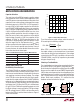
At CTRL voltages close to 1.225V, a soft transition occurs
between the CTRL pin and the internal reference. Figure 1
shows this behavior.
To set the maximum output voltage, select the values of
R1 according to the following equation:
R
V
k
OUT MAX
1 182
1 225
1=
⎛
⎝
⎜
⎞
⎠
⎟
•
.
–
()
Ω
When CTRL is used to override the internal reference,
the output voltage can be lowered from the maximum
value down to nearly the input voltage level. If the voltage
source driving the CTRL pin is located at a distance to the
LT3494/LT3494A, a small 0.1μF capacitor may be needed
to bypass the pin locally.
Choosing a Feedback Node
The single feedback resistor may be connected to the V
OUT
pin or to the CAP pin (see Figure 2). Regulating the V
OUT
pin eliminates the output offset resulting from the voltage
drop across the output disconnect PMOS. Regulating the
CAP pin does not compensate for the voltage drop across
the output disconnect, resulting in an output voltage V
OUT
that is slightly lower than the voltage set by the resistor
divider. Under most conditions, it is advised that the
feedback resistor be tied to the V
OUT
pin.
Figure 1. CTRL to FB Transfer Curve
SW CAP
V
CC
SHDN
CTRL
V
OUT
FB
GND
3
5
4
7
6
2
R1
LT3494
C1
C3
18
V
OUT
SW CAP
V
CC
SHDN
CTRL
V
OUT
FB
GND
3
5
4
7
6
2
R1
3494 F02
LT3494
C1
18
Figure 2. Feedback Connection Using the CAP Pin or the V
OUT
Pin
CTRL VOLTAGE (V)
0
0
FB VOLTAGE (V)
0.250
0.500
0.750
1.000
1.500
.25
0.5 .75 1.0
3494 F01
1.25 1.5
1.250