
Datasheet

LT3517
6
3517fg
For more information www.linear.com/LT3517
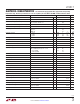
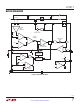
PIN FUNCTIONS
SW: Switch Pin. Minimize trace at this pin to reduce EMI.
V
IN
: Input Supply Pin. Must be locally bypassed.
SHDN: Shutdown Pin. Tie to 1.5V or higher to enable
device or 0.4V or less to disable device.
V
REF
: Reference Output Pin. This pin can supply up to
100µA.
RT : Switching Frequency Adjustment Pin. Set switching
frequency using a resistor to GND (see Typical Performance
Characteristics for values). For SYNC function, choose
the resistor to program a frequency 20% slower than the
SYNC pulse frequency. Do not leave this pin open.
SYNC: Frequency Synchronization Pin. Tie an external
clock signal here. R
T
resistor should be chosen to pro-
gram a switching frequency 20% slower than SYNC pulse
frequency. Synchronization (power switch turn-on) occurs
a fixed delay after the rising edge of SYNC. Tie the SYNC
pin to ground if this feature is not used.
SS: Soft-Start Pin. Place a soft-start capacitor here. Leave
the pin open if not in use.
PWM: Pulse Width Modulated Input Pin. Signal low turns
off channel, disables the main switch and makes the TG
pin high. Tie the PWM pin to V
REF
pin or SHDN pin if not
used. There is an equivalent 50k resistor from PWM pin
to ground internally.
CTRL: LED Current Adjustment Pin. Sets voltage across
sense resistor between ISP and ISN. Connect directly to
V
REF
for full-scale threshold of 100mV, or use signal values
between GND and 1V to modulate LED current. Tie the CTRL
pin to the V
REF
pin if not used.
VC: g
m
Error Amplifier Output Pin. Stabilize the loop with
an RC network or compensating C.
FB: Voltage Loop Feedback Pin. Works as overvoltage
protection for LED drivers. If FB is higher than 1V, the
main switch is turned off.
TGEN: Top Gate Enable Input Pin. Tie to 1.5V or higher
to enable the PMOS driver function. Tie the TGEN pin to
ground if TG function is not used. There is an equivalent
40k resistor from TGEN pin to ground internally.
ISN: Current Sense (–) Pin. The inverting input to the
current sense amplifier.
ISP: Current Sense (+) Pin. The noninverting input to the
current sense amplifier. Also serves as positive rail for
TG pin driver.
TG: Top Gate Driver Output. An inverted PWM sig-
nal drives series PMOS device between V
ISP
and
(V
ISP
– 7V). An internal 7V clamp protects the PMOS gate.
Leave TG unconnected if not used.
GND: Exposed Pad (QFN Package). Solder paddle directly
to ground plane.