
Datasheet


LT3581
19
3581fa
For more information www.linear.com/LT3581
ENABLE
1.5µH
1.5µH
6.8µF
4.7µF
4.7µF
2.2µF
100pF
SW1 SW2
GATE FB
V
C
SS
GND
SYNC
CLKOUTV
IN
RT
SHDN
FAULT
LT3581
SLAVE
SW1 SW2
GATE CLKOUT
V
C
SS
GND
SYNC
FBV
IN
RT
FAULT
SHDN
LT3581
MASTER
143k
V
OUT
–12V
450mA
V
IN
5V
V
OUT
12V
830mA
10k
10.5k
2.2nF
0.1µF
0.1µF
130k
43.2k
56pF
1nF
43.2k
100k
10k
3581 F11
6.8µF
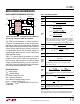
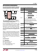
Figure 11. A Single Inductor Inverting Topology Is Synchronized
with a Boost Regulator to Generate –12V and 12V Outputs. The
External PMOS Helps Disconnect the Input from the Power Paths
During Fault Events
Also, the FAULT pins can be tied together so that a fault
condition from one LT3581 causes all of the LT3581s to
enter fault, until the fault condition disappears.
CHARGE PUMP AIDED REGULATORS
Designing charge pumps with the LT3581 can offer ef
-
ficient solutions with fewer components than traditional
cir
cuits because of the master/slave switch configuration
on the IC. Although the slave switch, SW2, operates in
phase with the master switch, SW1, it is only the current
through the master switch (SW1) that is sensed by the
current comparator (A4 in Block Diagram) as part of the
current feedback loop. This method of operation by the
master/slave switches can offer the following benefits to
charge pump designs:
applicaTions inForMaTion
Clock Synchronization
The operating frequency of the LT3581 can be set by an
external source by simply providing a digital clock signal
into the SYNC pin (R
T
resistor still required). The LT3581
will revert to its internal free-running oscillator clock (set
by the R
T
resistor) when the SYNC pin is driven below
0.4V for a few free-running clock periods.
Driving SYNC high for an extended period of time effec
-
tively stops the operating clock and prevents latch SR1
from becoming set (see Block Diagram). As a result, the
switching operation of the LT3581 will stop and the CLKOUT
pin will be held at ground.
The duty cycle of the SYNC signal must be between 20%
and 80% for proper operation. Also, the frequency of the
SYNC signal must meet the following two criteria:
(1) SYNC may not toggle outside the frequency range of
200kHz to 2.5MHz unless it is stopped low (below
0.4V) to enable the free-running oscillator.
(2) The SYNC frequency can always be higher than the
free-running oscillator frequency (as set by the R
T
resistor), f
OSC
, but should not be less than 25%
below f
OSC
.
CLOCK SYNCHRONIZATION OF ADDITIONAL
REGULATORS
The CLKOUT pin of the LT3581 can be used to synchronize
one or more other compatible switching regulator ICs as
shown in Figure 11.
The frequency of the master LT3581 is set by the external
R
T
resistor. The SYNC pin of the slave LT3581 is driven
by the CLKOUT pin of the master LT3581. Note that the
RT pin of the slave LT3581 must have a resistor tied to
ground. It takes a few clock cycles for the CLKOUT signal
to begin oscillating, and it’s preferable for all LT3581s to
have the same internal free-running frequency. Therefore,
in general, use the same value R
T
resistor for all of the
synchronized LT3581s.