
Datasheet


LT3591
11
3591f
APPLICATIONS INFORMATION
LOW INPUT VOLTAGE APPLICATIONS
The LT3591 can be used in low input voltage applications.
The input supply voltage to the LT3591 must be 2.5V or
higher. However, the inductor can be run off a lower battery
voltage. This technique allows the LEDs to be powered off
two alkaline cells. Most portable devices have a 3.3V logic
supply voltage which can be used to power the LT3591.
The LEDs can be driven straight from the battery, resulting
in higher effi ciency.
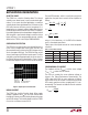
Figure 10 shows six LEDs powered by two AA cells. The
battery is connected to the inductor and the chip is powered
off a 3.3V logic supply voltage.
CTRL
V
IN
C2
4.7µF
C1: TAIYO YUDEN EMK107BJ105MA
C2: MURATA GRM31CR71H475KA12L
L1: TAIYO YUDEN NR4018T150M
C1
1µF
L1
15µH
C1
1µF
2 AA CELLS
2V TO 3.2V
3.3V
R
SENSE
10Ω
3591 F10
LT3591
SHUTDOWN AND
DIMMING CONTROL
SW
CAP
LED
GND
Figure 10. 2 AA Cells to Six White LEDs
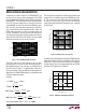
BOARD LAYOUT CONSIDERATIONS
As with all switching regulators, careful attention must be
paid to the PCB board layout and component placement.
To prevent electromagnetic interference (EMI) problems,
proper layout of high frequency switching paths is essential.
Minimize the length and area of all traces connected to
the switching node pin (SW). Keep the sense voltage pins
(CAP and LED) away from the switching node. Place C
OUT
next to the CAP pin. Always use a ground plane under the
switching regulator to minimize interplane coupling. Re-
commended component placement is shown in Figure 11.
Figure 11. Recommended Component Placement
L1
C
IN
C
OUT
3591 F11
V
IN
CTRL
LED
CAP
R
SENSE
SW
6
7
GND
9
8
3
2
1
5
4