
Datasheet


LT3591
5
3591f
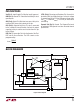
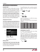
BLOCK DIAGRAM
PIN FUNCTIONS
V
IN
(Pin 1): Input Supply Pin. Must be locally bypassed.
GND (Pin 2): Ground Pin. Should be tied directly to local
ground plane.
SW (Pin 4): Switch Pin. Minimize trace area at this pin to
minimize EMI. Connect the inductor at this pin.
CAP (Pin 5): Output of the Driver. This pin is connected
to the cathode of internal Schottky. Connect the output
capacitor to this pin and the sense resistor from this pin
to the LED pin.
LED (Pin 7): Connection Point for the Anode of the First
LED and the Sense Resistor. The LED current can be
programmed by :
I
mV
R
LED
SENSE
=
200
CTRL (Pin 8): Dimming and Shutdown Pin. Connect this
pin below 50mV to disable the driver. As the pin voltage
is ramped from 0V to 1.5V, the LED current ramps from
0 to I
LED
( = 200mV/R
SENSE
). The CTRL pin must not be
left fl oating.
Exposed Pad (Pin 9): Ground. The Exposed Pad must
be soldered to PCB ground to achieve the rated thermal
performance.
4
–
+
–
+
R
SW
CAP
1
V
IN
Q
S
DRIVER
Σ
OVERVOLTAGE
PROTECTION
RAMP
GENERATOR
OSCILLATOR
V
REF
1.25V
START-UP
CONTROL
SHDN
Q1
R
–
+
+
5
LED
3591 F01
CTRL GND
7
82
–
+
A = 6.25
A1
R
C
C
C
A2
A3
PWM
COMP
Figure 1. Block Diagram