
Datasheet


LT3591
6
3591f
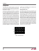
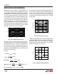
Figure 2. Switching Waveforms
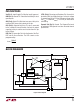
OPERATION
The LT3591 uses a constant frequency, current mode
control scheme to provide excellent line and load regula-
tion. Operation can be best understood by referring to the
Block Diagram in Figure 1.
At power-up, the capacitor at the CAP pin is charged up
to V
IN
(input supply voltage) through the inductor and
the internal Schottky diode. If CTRL is pulled higher than
100mV, the bandgap reference, the start-up bias and the
oscillator are turned on. At the start of each oscillator cycle,
the power switch Q1 is turned on. A voltage proportional
to the switch current is added to a stabilizing ramp and the
resulting sum is fed into the positive terminal of the PWM
comparator, A2. When this voltage exceeds the level at the
negative input of A2, the PWM logic turns off the power
switch. The level at the negative input of A2 is set by the
error amplifi er A1, and is simply an amplifi ed version of
the difference between the V
CAP
and V
LED
voltage and the
bandgap reference. In this manner the error amplifi er, A1,
sets the correct peak current level in inductor L1 to keep
the output in regulation. The CTRL pin is used to adjust
the LED current. The LT3591 enters into shutdown when
CTRL is pulled lower than 50mV.
Minimum Output Current
The LT3591 can drive a 2-LED string at 2mA LED current
without pulse skipping using the same external compo-
nents shown in the application circuit on the front page of
this data sheet. As current is further reduced, the device
will begin skipping pulses. This will result in some low
frequency ripple, although the average LED current remains
regulated down to zero. The photo in Figure 2 details circuit
operation driving two white LEDs at 2mA load. Peak induc-
tor current is less than 40mA and the regulator operates
in discontinuous mode, meaning the inductor current
reaches zero during the discharge phase. After the inductor
current reaches zero, the SW pin exhibits ringing due to
the LC tank circuit formed by the inductor in combination
with the switch and the diode capacitance. This ringing is
not harmful; far less spectral energy is contained in the
ringing than in the switch transitions.
V
SW
5V/DIV
I
L
20mA/DIV
V
IN
= 4.2V
I
LED
= 2mA
2 LEDs
500ns/DIV
3591 F02