
Datasheet


LT3743
20
3743fd
APPLICATIONS INFORMATION
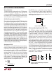
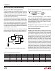
Average Current Mode Control Compensation
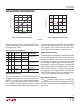
The use of average current mode control allows for precise
regulation of the inductor and LED currents. Figure
16
shows the average current mode control loop used in the
LT3743, where the regulation current is programmed by
a current source and a 3k resistor.
To design the compensation network, the maximum com-
pensation resistor needs to be calculated. In current mode
controllers, the ratio of the sensed inductor current ramp
to the slope compensation ramp determines the stability
of the current regulation loop above 50% duty cycle
. In
the same way, average current mode controllers require
the slope of the error voltage to not exceed the PWM ramp
slope during the switch off-time.
Since the closed-loop gain at the switching frequency
produces the error signal slope, the output impedance of
the error amplifier will be the compensation resistor, R
C
.
Use the following equations as a good starting point for
compensation component sizing:
R
C
=
f
S
• L • 1000V
V
O
• R
S
[Ω], C
C
=
0.002
f
S
[F]
where f
S
is the switching frequency, L is the inductance
value, V
IN
is the input voltage and R
S
is the sense resistor.
For most LED applications, a 4.7nF compensation capaci-
tor is adequate and provides excellent phase margin with
optimized bandwidth. Please refer to Table 6 for recom-
mended compensation values.
For applications where the load is not an LED, please call
the factory for additional compensation
assistance.
Board Layout Considerations
Average current mode control is relatively immune to the
switching noise associated with other types of control
schemes. Placing the sense resistor as close as possible
to the SENSE
+
and SENSE
–
pins avoids noise issues and
ensures the fastest LED current transition time. For currents
exceeding 5A, use 10Ω resistors in-series with SENSE
+
and SENSE
–
, with a 33nF capacitor placed as close as
possible to the SENSE
+
and SENSE
–
pins. Utilizing a good
ground plane underneath the switching components will
minimize interplane noise coupling. To dissipate the heat
from the switching components, increase the area of the
switching node as much as possible without negatively
affecting the radiated noise. The interconnect inductance
and resistance between the output capacitors and the LED
load directly impacts the rise
time of the load current. To
reduce the inductance and resistance, make the traces as
wide as physically possible and minimize the trace length.
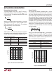
Table 6. Recommended Compensation Values
V
IN
(V) V
O
(V) I
L
(A) f
SW
(MHz) L (µH) R
S
(mΩ) R
C
(kΩ) C
C
(nF)
12 4 5 0.5 1.5 5 47.5 4.7
12 4 10 0.5 1.5 5 47.5 4.7
12 5 20 0.25 1.8 2.5 38.3 8.2
24 4 2 0.5 1.0 2.5 52.3 4.7
24 4 20 0.5 1.0 2.5 52.3 4.7
–
+
g
m
ERROR AMP
MODULATOR
LOAD
R
C
L R
S
3k
V
CTRL
• 11µA/V
C
C
3743 F16
Figure 16. LT3743 Average Current Mode Control Scheme